[News] TSMC Sees AI Wafer Demand Rising 11x From 2022–2026, Targets CoWoS With 24 HBM Stacks in 2029
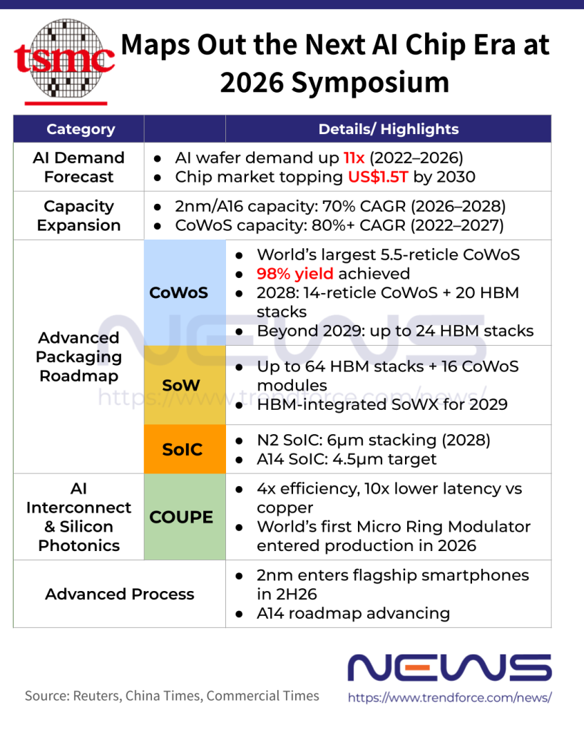
TSMC held its Taiwan Technology Symposium today. According to Reuters, the company said that demand for AI accelerator wafers is projected to grow 11-fold between 2022 and 2026. TSMC also raised its forecast for the global semiconductor market, now expecting it to exceed US$1.5 trillion by 2030, up from its previous US$1 trillion estimate.
According to Central News Agency, TSMC’s Asia-Pacific business head said customers in the region used more than 2.1 million 12-inch equivalent wafers last year, enough to surpass the height of three Taipei 101 towers if stacked vertically, underscoring surging AI demand.
TSMC said capacity for its most advanced 2nm and next-generation A16 chips is projected to grow at a 70% CAGR from 2026 to 2028, while CoWoS (Chip on Wafer on Substrate) advanced packaging capacity is forecast to achieve a CAGR of more than 80% from 2022 to 2027. The company also plans to build nine phases of wafer fabs and advanced packaging facilities in 2026, as noted by Reuters.
Notably, its Arizona operations continue ramping, with the first fab already in production, a second entering tool move-in in 2H26. Construction of a third fab is underway, and work on a fourth fab and the site’s first advanced packaging facility is expected to begin this year. According to TSMC, Arizona output is expected to increase 1.8-fold year over year by 2026, with yields comparable to Taiwan.
TSMC Highlights CoWoS, COUPE and SoW Roadmaps
Beyond capacity expansion, TSMC also outlined its long-term AI technology roadmap at the symposium. As noted by China Times, TSMC Deputy Co-COO Kevin Zhang said future AI accelerator performance will depend on the integration of transistor computing, advanced packaging, and high-speed interconnect technologies, with growing AI model sizes increasing the importance of SoIC and 3D IC technologies for directly stacking DRAM on compute chips.
In 3D stacking technology, TSMC’s SoIC continues to scale down. According to Commercial Times, SoIC has achieved 56 times higher interconnect density and five times better energy efficiency compared with 2015-era CoWoS. The report adds that first-generation SoIC has already entered mass production, while the 6-micron bonding pitch version is set for 2025. N2-generation SoIC will support 6-micron stacking in 2028, while the A14 generation is expected to advance further to 4.5-micron.
Regarding high-speed interconnects, Zhang said silicon photonics and TSMC’s COUPE (Compact Universal Photonic Engine) technology will be key to reducing latency and power consumption in future AI systems. According to Commercial Times, TSMC said that the world’s first 200Gbps Micro Ring Modulator using COUPE entered production this year. The technology delivers four times higher energy efficiency and 10 times lower latency than traditional copper interconnects.
As for CoWoS, Commercial Times notes that TSMC’s currently mass-produced 5.5-reticle-size version is the world’s largest today and has already achieved yields of 98%. The report adds that TSMC plans to rapidly scale CoWoS, targeting a 14-reticle-size version capable of integrating 20 HBM stacks in 2028, before moving beyond 14 reticles with support for up to 24 HBM stacks in 2029.
Beyond CoWoS, Commercial Times adds that TSMC is also advancing System on Wafer (SoW) technology, which can integrate up to 64 HBM stacks and 16 CoWoS modules at sizes exceeding 40 reticles. According to the report, logic-only SoWP entered mass production in 2024, while HBM-integrated SoWX is targeted for 2029.
Read more
- [News] TSMC Latest Roadmap: A12, A13 for 2029 Without High-NA EUV; A16 Volume Production Delayed to 2027
- [News] Behind TSMC’s High-NA EUV Deferral: Low-NA Stays Strong, Customer Landscape Shifts, and ASML Quietly Pivots
(Photo credit: TSMC)