[News] Musk’s Terafab Vision Raises Questions Over TSMC Impact; Advanced Packaging May be Best Entry Point
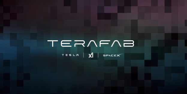
Tesla CEO Elon Musk has unveiled the Terafab mega-fab vision, aiming to integrate logic, memory, and advanced packaging, raising questions about potential pressure on foundry leader TSMC. According to Commercial Times, industry sources note that starting at the 2nm node would be extremely challenging for Terafab. However, if Tesla gradually enters the space through advanced packaging, supply chain integration, and partnerships with Samsung and Intel, it could still reshape global semiconductor supply chain dynamics over the long term.
As the report indicates, the biggest challenge for Terafab lies not in building the fab itself, but in controlling yields at advanced nodes. Entering the 2nm era, transistor architecture has shifted from FinFET to GAAFET, requiring broad upgrades in materials, equipment, and process modules, with even minor deviations at any stage potentially causing a sharp drop in yield. This underscores that competition in advanced-node fabs is not just about capital expenditure, but about long-accumulated process integration, defect databases, and experience curves, which remain TSMC’s core strengths.
In addition, equipment supply is another major barrier. The report indicates that advanced EUV lithography systems depend on a limited number of suppliers, with long lead times and high costs. Moreover, the U.S. still lags behind Asia in semiconductor engineering talent, fab construction experience, and supply chain maturity.
Advanced Packaging May Be Terafab’s Best Entry Point
Still, Terafab may hold potential to reshape parts of the value chain. As the report highlights, Tesla’s most likely entry point is advanced packaging. With part of the current AI chip bottleneck stemming from limited packaging capacity, Tesla could move first by leveraging packaging lines in Texas, panel-level packaging, or partnerships with external players to secure back-end capacity for its own AI chips, thereby reducing reliance on external supply chains.
From the perspective of its impact on TSMC, Terafab is unlikely to pose a meaningful threat to advanced-node leadership in the short term. However, over the medium to long term, if Tesla establishes a “partially in-house, partially collaborative” model, the real impact may be less on TSMC’s technological lead and more on large customers’ bargaining power within the supply chain. The report points out that even if Terafab does not become a fully integrated mega-fab, it could still serve as a strategic bargaining chip for Tesla to pursue greater chip autonomy.
Meanwhile, as noted by Tom’s Hardware, Musk said Tesla, SpaceX, and xAI will continue sourcing chips from existing suppliers such as TSMC, Samsung, and Micron, and expressed hope that they can expand capacity as quickly as possible. Musk did not provide a timeline for when Terafab would begin production or reach its target output, the report adds.
Terafab is expected to primarily produce two types of chips: one designed for electric vehicles and the Optimus humanoid robot, optimized for edge computing and inference; and another, the “D3” chip designed for space environments and low-Earth-orbit AI satellites, as noted by Economic Daily News.
Read more
- [News] Tesla Reportedly Weighs Doubling AI6 Output, May Add Samsung Orders Ahead of Executive Talks
- [News] Samsung Groq Orders May Jump ~70% to 15K Wafers; Tesla Reportedly Delays Other Foundry Clients
(Photo credit: Tesla on X)