Popular Keywords
About TrendForce News
TrendForce News operates independently from our research team, curating key semiconductor and tech updates to support timely, informed decisions.
[News] China Completed the World’s First 35-micron Ultra-Thin Wafer Process and Packaging & Testing Production Line
According to official sources from Shanghai’s Songjiang District, Nixi Semiconductor Technology (Shanghai) Co., Ltd., located in the Songjiang Comprehensive Bonded Zone, has officially completed the world’s first 35-micron ultra-thin wafer process and packaging & testing production line for power semiconductors. The project marks a major breakthrough for China in ultra-thin wafer manufacturing and advanced packaging for power devices, filling a long-standing domestic gap in both technology and production capacity.
The new line integrates the entire manufacturing chain including wafer bonding, grinding and thinning, laser dicing, and packaging and testing, representing the first globally to achieve mass production of 35-micron ultra-thin power semiconductor wafers through a fully integrated production platform. Led by Nixi Semiconductor, the facility is regarded as a major upgrade to the China production base of Alpha and Omega Semiconductor (AOS), enabling highly coordinated manufacturing from wafer processing to finished product testing.
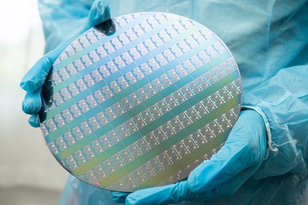
At just 35 microns thick—about half the diameter of a human hair—these ultra-thin wafers present significant manufacturing challenges. Once wafer thickness drops below 50 microns, mechanical fragility increases dramatically, placing stringent demands on precision processing and stress control.
Through joint development with equipment suppliers, the production line has achieved wafer thickness control of 35 ± 1.5 microns. A chemical etching process eliminates 92% of grinding-induced stress damage, while wafer breakage rates are kept below 0.1%. In the dicing stage, customized laser cutting replaces traditional blade dicing, greatly reducing the heat-affected zone and delivering a cutting yield of 98.5%, which are widely known as the key technical barriers in ultra-thin wafer processing.
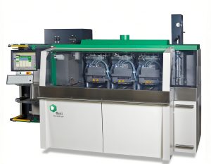
The production line is equipped with a full set of specialized manufacturing equipment. Bonding machines maintain alignment errors within 120 microns, with a daily capacity of about 400 wafers. Grinding systems achieve 0.1-micron precision, with intra-wafer thickness variation below 2 microns. The laser dicing system features a kerf width of just 11 microns, improving effective chip area utilization by approx. 10% compared with conventional blade cutting. In the testing stage, daily output can reach 120,000 finished devices, demonstrating the line’s capability for large-scale commercial production.
Notably, the line’s core equipment—including bonding, grinding, cutting, and debonding systems—was jointly developed by Nixi Semiconductor and Chinese domestic equipment manufacturers, which ensures independent control of critical manufacturing tools while filling a gap in China’s equipment applications for ultra-thin wafer production.
The new line is expected to significantly enhance the performance of power semiconductor devices. The ultra-thin wafer architecture can substantially reduce on-resistance and thermal resistance, shortening carrier transit time by 40%.
Thermal resistance drops by 60% compared with conventional 100-micron wafers, and when combined with a double-sided heat dissipation packaging design, module-level thermal resistance can be reduced by a further 30%, while power cycling lifetime increases fivefold.
These improvements will markedly enhance the energy efficiency and thermal performance of power devices, targeting high power-density applications such as new energy vehicles and 5G base stations, and providing mass-production support for domestically manufactured power devices entering high-voltage and fast-charging markets.
Nixi Semiconductor was founded in 2007 and is one of the primary semiconductor manufacturing bases of Alpha and Omega Semiconductor (AOS) in China. The company is wholly owned by Alpha and Omega Semiconductor (Hong Kong) Co., Ltd., and the completion of this new production line is expected to further strengthen its core competitiveness in power semiconductor manufacturing.
(Photo credit: FREEPIK)