Popular Keywords
About TrendForce News
TrendForce News operates independently from our research team, curating key semiconductor and tech updates to support timely, informed decisions.
[News] NAND Giant YMTC Reportedly Debuts First Commercial PCIe 5.0 SSD Using In-house Xtacking Flash
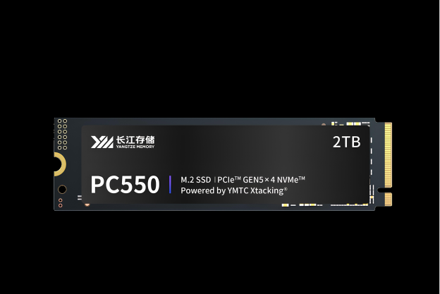
Amid the ongoing global memory shortage, Chinese memory makers are pushing aggressively to capture a bigger slice of the market. According to Tom’s Hardware, YMTC, the nation’s NAND heavyweight, has officially entered the PCIe 5.0 SSD arena with its first commercial offering, the PC550.
According to YMTC, PC550 is a PCIe 5.0 commercial SSD purpose-built for AI PCs. Product details on its website further reveal that the PC550 uses the company’s in-house X4-9070 3D NAND built on Xtacking 4.0., and its four-channel design is engineered to reduce heat and power consumption.
Tom’s Hardware, citing company disclosures, also notes that the drive comes in 512GB, 1TB, and 2TB variants, compatible with M.2 2242 and 2280 slots, with the top-tier 2TB model hitting peak speeds of 10,500 MB/s read and 10,000 MB/s write.
Though YMTC’s official PC550 SSD page doesn’t list pricing or direct purchase options, prospective buyers can submit an inquiry to express interest in the drive.
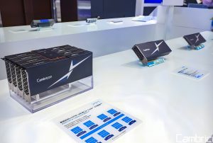
Notably, YMTC, with its consumer brand ZHITAI, has released a series of products in the past few months. In January, ZHITAI officially launched the 4TB version of its ZHITAI Ling Pioneer Edition portable SSD, which also features native flash memory chips based on YMTC’s Xtacking architecture. Equipped with a USB 3.2 Gen2x2 interface, it delivers sequential read and write speeds of up to 2,000 MB/s—allowing a 10GB HD video transfer in under five seconds—dramatically cutting file transfer time and boosting everyday productivity, according to its press release.
As highlighted by YMTC, before the introduction of the Xtacking architecture, 3D NAND designs in the industry were largely split between traditional side-by-side layouts and the CMOS-next-to-Array (CnA) approach.
After nearly a decade of development and four years of 3D IC validation, YMTC introduced a new method that bonds two wafers to form its 3D NAND flash. The company said that using an innovative layout, memory cells and peripheral circuits are connected through billions of metal VIAs (Vertical Interconnect Accesses) within a die roughly the size of a fingernail, while maintaining bonding reliability comparable to structures built on a single wafer.

(Credit: YMTC)
Read more
(Photo credit: YMTC)
Please note that this article cites information from Tom’s Hardware and YMTC.