Popular Keywords
- About Us
-
Research Report
Research Directory
Semiconductors
LED
Consumer Electronics
Emerging Technologies
- Selected Topics
- Membership
- Price Trends
- Press Center
- News
- Events
- Contact Us
- AI Agent
About TrendForce News
TrendForce News operates independently from our research team, curating key semiconductor and tech updates to support timely, informed decisions.
- Home
- News
[News] SK hynix Unveils AI Chip Architecture with HBF, Reportedly Boosts Performance per Watt by Up to 2.69×

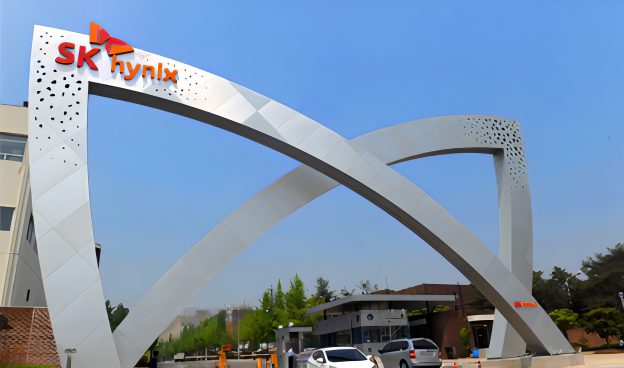
SK hynix has unveiled a new semiconductor architecture concept centered on High Bandwidth Flash (HBF), a memory technology that stacks multiple NAND flash dies. According to Hankyung, the company recently outlined the concept—dubbed “H3”—in a paper presented at the Institute of Electrical and Electronics Engineers (IEEE). H3 refers to a hybrid architecture that integrates both HBM and HBF into a single design.
As the report notes, the H3 architecture places both HBM and HBF alongside the GPU responsible for computation, whereas in current AI chips—including NVIDIA’s Rubin platform set for release in the second half of this year—only HBM is positioned next to the GPU.
To assess the feasibility of the H3 design, SK hynix carried out simulation tests. In these trials, the company configured eight fifth-generation HBM (HBM3E) stacks and eight HBF stacks alongside NVIDIA’s latest GPU, the Blackwell (B200). The simulations indicated that performance per watt improved by as much as 2.69× compared with setups relying solely on HBM, as the report highlights.
H3 Architecture with HBF May Boost AI Inference Performance
Notably, as the report points out, the H3 architecture is viewed as especially well-suited for AI inference, an area of growing importance. Inference refers to a model’s ability to reason and generate responses, and a central element of this process is the KV cache, which temporarily stores conversational context during user interactions.
The report explains that as AI models grow more sophisticated, KV cache requirements are expanding to levels that strain HBM and GPUs, potentially limiting overall computational efficiency. By deploying HBF as an additional high-capacity storage layer to absorb the KV cache, the GPU and HBM can be freed from storage overhead and concentrate on high-speed processing and generating new outputs.
SK hynix also simulated scenarios in which HBF handled a massive KV cache of up to 10 million tokens. According to the report, the simulations showed that the system’s capacity to process simultaneous queries (batch size) rose by as much as 18.8× compared with HBM-only setups. Workloads that previously required 32 GPUs could be executed with just two GPUs, resulting in substantially improved power efficiency.
Technical Challenges to HBF Commercialization
Through the paper, the company underscored HBF’s potential as a next-generation AI memory solution. However, as the report highlights, several challenges remain before commercialization. Although NAND flash offers high storage density, its relatively slow write performance, particularly when adding or modifying data, remains a key limitation.
Even if HBF is primarily used for read-intensive workloads within the hybrid architecture, write performance is becoming increasingly important for KV cache applications. The report notes that overcoming this limitation will require more advanced design, including significantly improving the controller performance of the base die at the bottom of the HBF stack.
Still, as HBF gains momentum in AI memory, standardization efforts are intensifying. According to Sisa Journal, Samsung Electronics and SK hynix have signed memorandums of understanding (MOUs) with SanDisk to advance HBF standardization and are now pursuing those efforts through a joint consortium. Both companies are actively developing HBF products, targeting commercialization by 2027.
Read more
- [News] Expert Says HBF May Be Deployed in NVIDIA GPUs by 2027–28; Market Could Surpass HBM by 2038
- [News] SLC-Based AI SSDs Gain Traction as SK hynix and Kioxia Accelerate Development With NVIDIA
(Photo credit: SK hynix)


