Popular Keywords
About TrendForce News
TrendForce News operates independently from our research team, curating key semiconductor and tech updates to support timely, informed decisions.
[News] TSMC Flags Significantly Higher Capex Over Next 3 Years; Arizona 4th Fab, Packaging Site in Works

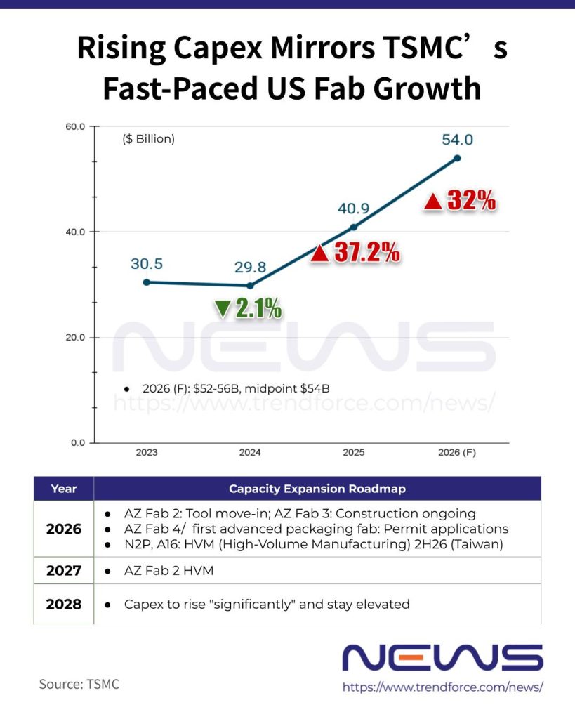
Even as TSMC stunned the market by guiding 2026 capital spending at US$52 billion to US$56 billion — a roughly 30% year-over-year jump — the company made clear that this is not the peak. CFO Wendell Huang noted that over the past three years, TSMC has invested roughly US$101 billion in capex, and that spending over the next three years will be “significantly higher,” though he did not provide specific figures.
According to Huang, TSMC’s capital spending totaled US$40.9 billion in 2025 and US$29.8 billion in 2024.
However, as new capacity typically takes several years to reach volume production, Chairman C.C. Wei noted that this year’s planned capex is expected to contribute little to 2026 output and only marginally to 2027. To address supply-demand gaps, the company will prioritize near-term output gains through productivity improvements rather than relying on new fabs coming online, he added.
Looking further ahead, Wei said capital spending will ramp up significantly from 2028 onward and remain elevated as long as the AI-driven demand cycle continues.
US Fab Acceleration Mirrors TSMC’s Overall Capex Push
Notably, TSMC’s aggressive capital spending mirrors the fast-paced expansion of its Arizona production hub. During the 4Q25 earnings call, Chairman and CEO C.C. Wei highlighted the company’s recent US$197 million purchase of an additional land parcel in Arizona, signaling plans for multiple fabs to better serve U.S. customers.
Wei outlined the Arizona roadmap, highlighting that the first fab has been in high-volume production since 4Q24. The second fab is now complete, with tool move-in scheduled for 2026 and high-volume output expected in the second half of 2027. According to TechNews citing Wei, construction on a third fab is already underway, while the company is seeking permits for a fourth fab and its first advanced packaging facility in the state.
On the other hand, in Taiwan, Wei pointed out that TSMC is planning a multi-phase 2nm wafer fab across its Hsinchu and Kaohsiung Science Parks, with ongoing investments planned for advanced process nodes and advanced packaging facilities.
He highlighted that TSMC’s N2 process began volume production in Q4 2025 at its Hsinchu and Kaohsiung fabs, achieving strong yields. The N2P variant, which offers better performance, is expected to enter volume production in the second half of 2026. Meanwhile, the A16 node, featuring best-in-class SPR (Super Power Rail), is also slated for volume production in H2 2026.
Together, N2, N2P, and A16 represent another large, long-lasting technology node for TSMC, underpinning the company’s roadmap for advanced, high-performance chips, Wei added.
Read more
- [News] TSMC Q1 Revenue Guidance Hits $35.8B, Up 38% YoY; Unveils Record $56B Capex for 2026
- [News] TSMC 2025 Q4 Net Profit Soars 35% YoY to Record NT$505.7B, EPS Hits NT$19.5
(Photo credit: TSMC)