Popular Keywords
About TrendForce News
TrendForce News operates independently from our research team, curating key semiconductor and tech updates to support timely, informed decisions.
[News] TSMC Reportedly Plans Mature-Node Tool Shift to Singapore, Accelerates Exit as Arizona Expands

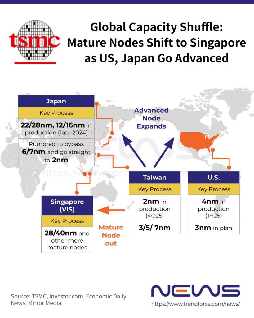
As TSMC steps up its Arizona push with a US$197 million land purchase for a future gigafab, the foundry is also reshaping capacity at home — trimming mature-node output to make room for more advanced processes. According to the Economic Daily News and Investor.com, it is considering shifting some mature-node tools in Taiwan to affiliate Vanguard International Semiconductor’s 12-inch fab in Singapore.
Investor.com, citing industry sources, reports that TSMC is not only relocating related chipmaking tools but also cutting 12-inch mature-node output, shifting some high-end power management orders to Vanguard’s Singapore fab and repurposing the freed-up space for 2nm and 3nm lines.
The report adds that in advanced packaging, the company is turning its focus to higher-margin lines, including CoW (Chip-on-Wafer) within CoWoS (Chip-on-Wafer-on-Substrate), as well as SoIC (System on Integrated Chips) and SOW (System on Wafer). TSMC has also asked its backend partners to clear space to take over test equipment being relocated, the report notes.
If so, it would mark another step by TSMC to free up room for more advanced capacity. Mirror Media reported earlier that the company submitted an internal proposal suggesting its Kumamoto Fab 2 in Japan could bypass 6nm and go straight to 2nm, targeting major AI customers such as NVIDIA and AMD.
Strategic Implications
Investor.com notes that strong demand for advanced nodes and packaging, combined with long lead times for new fabs and land and environmental hurdles, is driving TSMC’s plans. In addition, the Innolux plant acquired in 2024 is reportedly ill-suited for semiconductor production, requiring extensive retrofitting. With revenue growth targets in mind, expanding higher-margin advanced capacity is seen as the most efficient way to sustain a long-term gross margin above 53%, the report adds.
Meanwhile, the Economic Daily News observes that if the shift goes ahead, TSMC’s remaining mature-node operations are expected to focus increasingly on specialty processes, which could make up over 80% of its mature-node mix, supporting a one-stop supply model for advanced customers.
On the other hand, Commercial Times reports that TSMC announced on January 8 that the newly acquired Arizona site spans about 3.65 million square meters (roughly 110 hectares), in line with Chairman C.C. Wei’s plan to secure a second large plot near its fab for a standalone “gigafab” cluster, supporting aggressive investment to meet growing demand for high-end chips.
Since announcing its first US fab in May 2020, TSMC has steadily expanded its Arizona footprint. In March 2025, it raised its total planned US investment to US$165 billion, aiming for six wafer fabs, two advanced packaging facilities, and one R&D center.
Read more
- [News] TSMC Reportedly Suspends New 3nm Kick-offs, Steers Customers to 2nm to Optimize Costs
- [News] TSMC’s Bold Pivot: Kumamoto Fab 2 Reportedly Leaps from 6nm to 2nm amid JASM Losses
(Photo credit: TSMC)
Please note that this article cites information from Investor.com, Economic Daily News, Mirror Media, and Commercial Times.