Popular Keywords
- About Us
-
Research Report
Research Directory
Semiconductors
LED
Consumer Electronics
Emerging Technologies
- Selected Topics
- Membership
- Price Trends
- Press Center
- News
- Events
- Contact Us
- AI Agent
About TrendForce News
TrendForce News operates independently from our research team, curating key semiconductor and tech updates to support timely, informed decisions.
- Home
- News
[News] SK hynix Reportedly Plans First U.S. 2.5D Packaging Line, Eyes Turnkey HBM to Challenge TSMC

As SK hynix continues to advance next-generation memory, the company is also reportedly moving to build capabilities in cutting-edge packaging technologies. According to ZDNet, sources say SK hynix is preparing to set up its first 2.5D packaging mass-production line at a new U.S. packaging facility in West Lafayette, Indiana. 2.5D packaging improves chip performance and power efficiency by placing a thin silicon interposer between the semiconductor and the substrate, the report adds.
As the report notes, the West Lafayette packaging plant will be SK hynix’s first manufacturing facility in the U.S. and is intended to serve as an advanced packaging production hub for AI memory. The company is targeting the second half of 2028 for the start of operations and has announced plans to invest US$3.87 billion (around KRW 5.4 trillion) in the project.
2.5D Packaging Capabilities Could Redefine AI Supply Dynamics
2.5D packaging is a critical process for integrating HBM with high-performance system semiconductors, the report notes. It adds that NVIDIA’s high-performance AI accelerators are built by combining HBM with GPUs and CPUs through 2.5D packaging, making the technology central to advanced AI chip design.
To receive usage approval from NVIDIA, the report notes that quality validation must cover not only the HBM itself but also the 2.5D packaging process. This requirement means that any weaknesses in packaging can delay product timelines, even if the memory itself meets reliability standards. The report also notes that by further strengthening its technological capabilities, SK hynix could move toward a turnkey business model that offers customers both HBM and packaging in a single, integrated solution.
Against this backdrop, the report points out that SK hynix’s push to establish a 2.5D packaging mass-production line is part of a broader strategy to strengthen its overall AI semiconductor packaging capabilities, including HBM. If the company secures both the technology and large-scale manufacturing capacity for 2.5D packaging, the report adds, the move could significantly reshape the AI chip supply chain.
2.5D Packaging Seen as Key to SK hynix’s Commercial Expansion
SK hynix has been conducting in-house research and development on 2.5D packaging for an extended period. However, the report indicates that the company currently lacks sufficient domestic equipment to carry out the full 2.5D packaging process at mass-production scale. The report also points out that 2.5D packaging for AI accelerators is effectively dominated by TSMC.
While SK hynix has basic 2.5D packaging technology and equipment in place, sources say it remains difficult to support the large-scale system-in-package (SiP) tools required for AI accelerators integrating HBM. As a result, SK hynix views securing in-house facilities capable of performing 2.5D packaging for its own HBM as a key priority, with the aim that once the technology stabilizes and is further refined, the company can pursue business expansion beyond R&D.
SK hynix stated that it is exploring various options regarding the utilization of the Indiana fab, but nothing has been finalized at this stage.
Read more
- [News] SK hynix Reportedly Expands U.S. Footprint with New Seattle Office Near NVIDIA and Amazon
- [News] SLC-Based AI SSDs Gain Traction as SK hynix and Kioxia Accelerate Development With NVIDIA
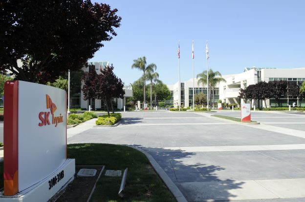
(Photo credit: SK hynix)


