Popular Keywords
About TrendForce News
TrendForce News operates independently from our research team, curating key semiconductor and tech updates to support timely, informed decisions.
[News] Rapidus Reportedly to Unveil Glass Substrate Interposer Prototype, Eyes 2028 Production
As SEMICON Japan opens today (December 17), Nikkei reports that semiconductor heavyweights—including NVIDIA, Intel, Micron, and TSMC—are set to participate. Yet the biggest buzz may center on Rapidus, the Japanese foundry expected to unveil the world’s first interposer prototype cut from a single large glass substrate, with mass production slated for 2028, according to Nikkei.
In July, Rapidus had produced its first 2nm transistor, targeting 2nm mass production by fiscal 2027. Now, with its interposer breakthrough, the company is making a bold push into back-end production, aiming to cut costs for AI semiconductor assembly, Nikkei points out.
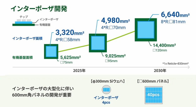
While TSMC mainly relies on silicon interposers for its CoWoS advanced packaging, Rapidus is taking a different route. The Japanese foundry uses a 600 mm square glass substrate, and its larger, low-waste design can yield up to 10 times more interposers per sheet than conventional 300 mm round silicon wafers, Nikkei reports.
It is worth noting that Rapidus is leveraging Japan’s extensive LCD expertise, recruiting engineers from Sharp and other display makers to tackle the challenges of working with fragile glass, which can crack or warp as panel sizes increase, Nikkei reports. Prototyping kicked off in June at the company’s cleanroom in Chitose, northern Japan, the report adds.
The Rapidus prototype, as per Nikkei, offers 30% to 100% more surface area than conventional interposers, accommodating larger chips. On top of that, glass provides better electrical performance than silicon, giving the design an additional edge, the report explains.
Rapidus has confirms on its website that it is setting up a cleanroom at Seiko Epson’s Chitose facility and launching a semiconductor back-end R&D center, “Rapidus Chiplet Solutions” (RCS). The center will focus on 2 nm-generation chiplet package design and manufacturing, supporting FCBGA, Si interposer, RDL, and hybrid bonding processes, and advancing mass-production technologies including automation.
Foundry Giants’ Glass Substrate Progress
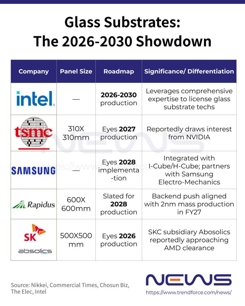
Currently, Intel, which has been developing the technology for more than a decade, remains the forerunner in the glass substrate sector. According to ETNews, the company is sticking to its 2023 roadmap, with pilot line operations set to begin in 2025. According to the plan cited by the report, Intel aims to roll out glass substrates ahead of 2030.
On the other hand, Commercial Times reports that TSMC, a leader in AI chip packaging with CoWoS, is ramping up efforts in glass substrates as well. The company has reportedly established dedicated R&D teams and lines for FOPLP (panel-level fan-out packaging) and is investing in PLP (Panel Level Packaging) and TGV (Through-Glass Via) technologies. While mass production was initially planned for 2027, supply chain sources indicate the timeline could be accelerated, the report adds.
Meanwhile, Samsung is accelerating its push toward glass substrates as well, aiming to use them for advanced semiconductors by 2028, The Korea Herald reports. Business Post adds that Samsung is considering investing in Intel’s packaging business, with potential collaboration extending to next‑generation glass substrates.
Read more
(Photo credit: Rapidus)
Please note that this article cites information from Nikkei, ETNews, Commercial Times, The Korea Herald, Business Post and Rapidus.