Popular Keywords
About TrendForce News
TrendForce News operates independently from our research team, curating key semiconductor and tech updates to support timely, informed decisions.
[News] China Guangdong to Build World’s Largest 12-Inch Optical SiC Production Base
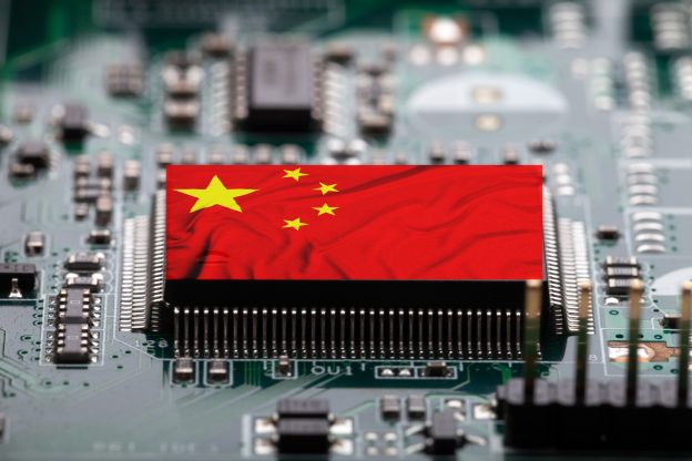
On November 19, China’s Shenzhen Kuotan Semiconductor Technology (Huizhou Huishikang Technology) announced plans to invest RMB 1.15 billion to build the world’s largest 12-inch optical-grade silicon carbide (SiC) materials production base in Zhongkai district, Huizhou, Guangdong.
The project covers 30,000m², with an annual capacity target of 200,000 wafers and projected yearly output value exceeding RMB 3.6 billion. Positioned directly at the high-end optical waveguide material segment, the initiative aims to break long-standing foreign monopolies and establish a domestically sourced materials foundation for AI chips, quantum communications, and AR/VR devices.
Huizhou Huishikang Technology was incorporated on 17 September 2025. Labeled as a “subsidiary under Kuotan Semiconductor,” the company was clearly set up specifically for the Zhongkai project.
Kuotan Semiconductor (Huizhou Huikang) achieved the transition from 8-inch to 12-inch wafers in just two years. In June 2022, the firm developed China’s Bay Area’s first 8-inch SiC substrate, which was soon validated by major global chipmakers. This August, its 12-inch SiC optical waveguide material rolled off the line in Huizhou, placing the company among a small group worldwide capable of producing both large-diameter conductive and high-purity single-crystal SiC.
According to Chairman Yao Yongxing, the new material, characterized by low absorption, high transmittance, and an ultra-high refractive index of 2.7, is one of the most advanced optical materials known today. It is designed to meet AR/AI glasses demands for ultra-thin form factors while supporting the stringent optical requirements of high-speed optical communications, LiDAR, and quantum communication chips.
Phase I of the project involves a RMB 300m investment to construct an optical-grade 12-inch SiC production line with a planned capacity of 50,000 wafer annually within one year. Products will include optical waveguide materials and CoWoS advanced-packaging interposer layers, serving AR/VR optical waveguide lenses, high-speed optical communications, LiDAR, and 2.5D/3D advanced packaging for AI chips and GPUs. While the company has not disclosed further investment or capacity ramp-up details, its overarching goal is clear: to establish a 200,000-wafer-per-year operation in Zhongkai with RMB 3.6 billion annual output—making it the world’s largest production base for 12-inch SiC materials.
(Photo credit: FREEPIK)