Popular Keywords
About TrendForce News
TrendForce News operates independently from our research team, curating key semiconductor and tech updates to support timely, informed decisions.
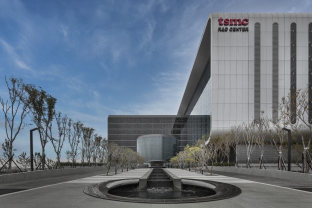
[News] TSMC Reportedly to Break Ground 1.4nm Taichung Fab on Nov. 5; Mass Production Slated in 2H28
Fresh off celebrating the first NVIDIA Blackwell wafer produced in Arizona, TSMC is ramping up its 1.4nm expansion in Taiwan. According to Economic Daily News, the company filed construction plans with the Central Taiwan Science Park Administration on October 17 and plans to break ground on November 5, with construction bidding already in full swing.
The new 1.4nm fab, slated for mass production in the second half of 2028, involves an estimated US$49 billion (NT$1.5 trillion) investment and is expected to create 8,000–10,000 jobs, the report says. Citing a statement from the Taichung City Government, Focus Taiwan adds that the fab could generate up to US$15.9 billion (NT$485.7 billion) in annual output.
Notably, as the Economic Daily News highlights, TSMC had initially planned four fabs at its Taichung site, with the first two in Phase 1 dedicated to 1.4nm production and Phase 2 potentially advancing to A10 (1nm). But as market attention toward 1.4nm technology intensifies, the report now suggests all four fabs may adopt the 1.4nm process, while 1nm production could be shifted to Shalun in the Southern Taiwan Science Park.
The report points out that TSMC’s push may come in response to Intel and Samsung’s rapid advances—with SoftBank and NVIDIA taking stakes in Intel to back its next-gen process development, while Samsung races to speed up 1.4nm mass production. Analysts cited in the report say TSMC’s accelerated 1.4nm expansion is aimed at cementing its lead in the tightening global race for next-generation chip technology.
While TSMC Chairman C.C. Wei said last week that the company will accelerate 2nm deployment in Arizona, Economic Daily News reports that the U.S. site will likely focus on 2nm to 1.6nm, keeping 1.4nm production centered in Taiwan. Once all four Taichung fabs are operational, the site is expected to become the world’s largest hub for AI and HPC chip production, the report adds.
Taichung Fabs Set to Drive Massive EUV Deployment
However, as Commercial Times reported, TSMC’s A14 process will not adopt High-NA EUV lithography; instead, it will continue using mature 0.33 NA EUV paired with more complex multi-patterning techniques. Analysts cited by the report said TSMC’s approach reflects a focus on cost control and proven technical maturity.
Nonetheless, TSMC’s appetite for EUV machines remains strong. Commercial Times reports that TSMC’s EUV tool demand is expected to exceed 30 units in 2027, reportedly in preparation for mass production at its Taichung fabs.
Read more
- [News] TSMC Confirms N2P for 2H26, Joins A16 to Cement 2nm-Class as Major, Long-Lived Node
- [News] TSMC Posts Record Q3 Profit, EPS NT$17.44 Amid AI Surge, Tariff Concerns
(Photo credit: TSMC)
Please note that this article cites information from Economic Daily News, Focus Taiwan and Commercial Times.