Popular Keywords
About TrendForce News
TrendForce News operates independently from our research team, curating key semiconductor and tech updates to support timely, informed decisions.
[News] Samsung 12H HBM3e Reportedly Clears NVIDIA Tests After 18-Month Setback, HBM4 Reaches Final Phase
After a year and a half of setbacks, Samsung has finally closed the gap with other memory giants. Multiple South Korean outlets, including the Korean Economic Daily and Business Korea, report that the company has cleared NVIDIA’s quality validation for its 12-high HBM3e, following its development last February.
Analysts cited by the Korean Economic Daily say the achievement reflects both Samsung’s performance upgrades to its existing HBM3e lineup and NVIDIA’s push to diversify its supplier base. According to the report, the 12-high chips are designed with 12 DRAM layers to maximize bandwidth and power the latest AI accelerators, including NVIDIA’s B300 and AMD’s MI350.
On the other hand, Aju News offers a slightly different perspective on Samsung’s HBM3e progress. The report notes that the company recently completed a second round of internal Wafer Acceptance Tests (WAT) on its 12-high HBM3E for NVIDIA, with results expected within days.
While strong WAT results are considered a positive sign that the chips could pass NVIDIA’s official qualification, the report emphasizes that Samsung has not yet received NVIDIA’s formal approval. As one industry insider cited by the report put it, “If NVIDIA’s qualification is the college entrance exam, Samsung’s WAT is the mock test using the same exam paper.”
In any case, the Korean Economic Daily highlights that Samsung’s breakthrough came from directly tackling the heat issue. The report credits Vice Chairman Jun Young-hyun, who took over the semiconductor division last May, for personally pushing a redesign. After meeting with NVIDIA’s leadership earlier this year, he reportedly instructed the development team to rework the 1a DRAM for HBM3e, paving the way for the company to finally clear the hurdle.
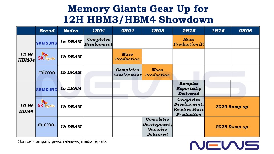
In comparison, SK hynix announced back in September, 2024, that it has begun mass production of the world’s first 12-layer HBM3e product with 36GB. Meanwhile, Business Korea reported in February that after the completion of development and sample delivery to clients in last September, Micron began mass production of 12-layer HBM3e in early 2025.
Samsung Accelerates HBM4 Race
While SK hynix announced in September that it has completed HBM4 development and is preparing for mass production, Aju News reports that Samsung is also making solid progress. The company recently cleared the Product Validation Review (PVR) stage for HBM4, one of the final steps in its new product development process, the report explains.
As the report notes, Samsung had already shipped HBM4 samples in the second quarter, but it is now dedicating its semiconductor division’s full resources to developing a revised version that incorporates NVIDIA’s performance improvement requirements.
The report suggests that 12-high HBM4 built on Samsung’s 1c DRAM chips is expected to outperform HBM4 products from SK hynix and Micron, which use 1b DRAM chips, allowing Samsung to effectively achieve NVIDIA’s requested bandwidth of 10Gbps per chip.
TrendForce reports that NVIDIA has recently pressed key component suppliers of its Vera Rubin server racks to upgrade product specifications, specifically requesting that HBM4 speed per pin be raised to 10 Gbps, as AMD gets set to launch its MI450 Helios platform in 2026.
Among the three leading suppliers, Samsung took an aggressive step in 2024 by upgrading the HBM4 base die process node to FinFET 4nm, targeting volume production by the end of the year, according to TrendForce.
Read more
- [News] Samsung Reportedly Passes NVIDIA HBM4 Sample Test, 30% HBM3E Discount to Challenge SK hynix
- [News] HBM Battle Heats Up: Micron Reportedly Hints 2026 Sell-Out, SK hynix Yet to Confirm
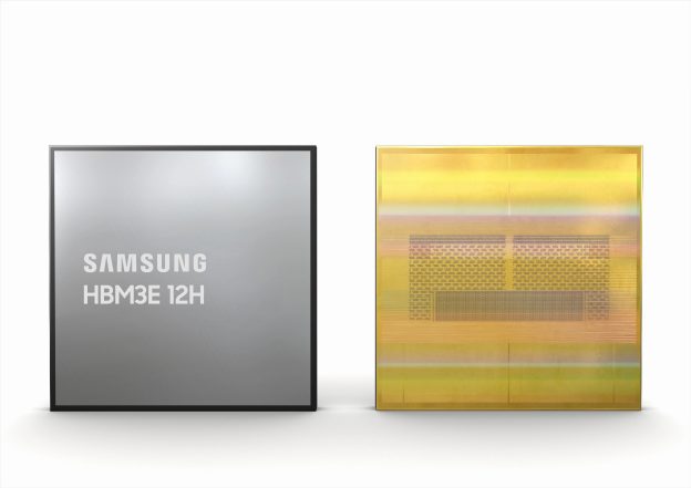
(Photo credit: Samsung)
Please note that this article cites information from Korean Economic Daily, Business Korea, Aju News, and SK hynix.