Popular Keywords
- About Us
-
Research Report
Research Directory
Semiconductors
LED
Consumer Electronics
Emerging Technologies
- Selected Topics
- Membership
- Price Trends
- Press Center
- News
- Events
- Contact Us
- AI Agent
About TrendForce News
TrendForce News operates independently from our research team, curating key semiconductor and tech updates to support timely, informed decisions.
- Home
- News
[News] Researchers Propose “Beyond EUV” Using Soft X-Rays, Potentially Challenging High-NA EUV

According to Tom’s Hardware, citing Cosmos, Johns Hopkins University researchers have proposed “beyond-EUV (B-EUV),” a step beyond today’s industry-standard EUV lithography. The method employs 6.5–6.7nm soft X-ray lasers, which the report notes could enable resolutions down to 5nm and below.
To put this into context, today’s most advanced chips are manufactured using EUV lithography, which operates at a 13.5nm wavelength. As the report notes, depending on the optical setup, the process can achieve feature sizes of about 13nm with Low-NA EUV, 8nm with High-NA, and as small as 4–5nm with Hyper-NA. Notably, B-EUV could potentially push resolution even further, to 5nm and below.
As the report points out, Johns Hopkins University researchers show that using a shorter wavelength provides an intrinsic resolution boost, even with lenses of only moderate NA. However, the researchers admit they are still years from building even a prototype B-EUV tool, with the study published in Nature Chemical Engineering.
Key Challenges of B-EUV
As the report notes, while B-EUV might in theory compete with Hyper-NA EUV, its development remains highly challenging.
One of the biggest obstacles is the light source. Researchers have explored several methods to generate 6.7nm radiation, such as gadolinium laser-produced plasma, but, as the report points out, no reliable solution has yet been achieved.
Another challenge lies in the interaction of these shorter wavelengths with materials. Their high photon energy makes them incompatible with conventional photoresists used in chipmaking. In addition, 6.5–6.7nm light is absorbed by nearly all materials, creating the need for multilayer-coated mirrors designed specifically for this radiation.
Finally, as the report highlights, there is still no supporting ecosystem of components and consumables like pellicles or photomasks to enable the design and deployment of B-EUV lithography tools.
Progress in Materials and Processes for B-EUV
Despite these challenges, the research addresses one issue through the use of new materials. As the report notes, the team explored how certain metals, such as zinc, could enhance the interaction between B-EUV light (around 6nm wavelength) and the resist materials used in chipmaking. The report adds that while zinc is well suited for B-EUV, the team noted other metals may perform better at different wavelengths, offering greater flexibility for future chipmaking technologies.
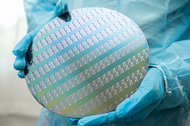
In addition, the researchers devised a technique called chemical liquid deposition (CLD) to apply these metal–organic compounds onto silicon wafers. This approach forms thin, mirror-like layers of a material known as aZIF (amorphous zeolitic imidazolate frameworks), growing at a rate of 1nm per second.
Read more
- [News] Tsinghua University Breaks Ground on EUV Photoresist in China’s Semiconductor Push
- [News] SMIC Said to Test Chinese-Made DUV Lithography Tool from SiCarrier Affiliate Amid AI Chip Push
(Photo credit: FREEPIK)


