Popular Keywords
About TrendForce News
TrendForce News operates independently from our research team, curating key semiconductor and tech updates to support timely, informed decisions.
[News] NVIDIA May Be Among the First to Adopt TSMC A16 for 2028 Feynman Architecture
According to Commercial Times, sources say NVIDIA is weighing the adoption of TSMC’s most advanced process, the A16 — a 2nm-class node with backside power delivery slated for mass production in the second half of 2026. In 2026, alongside major smartphone makers adopting TSMC’s 2nm, AMD is set to launch HPC (high-performance computing) chips on the node. To counter AMD’s early move, the report highlights that NVIDIA may be among the first to adopt A16, with plans to use it in its upcoming Feynman architecture. This would mark a key turning point, as it would be the first time AI applications lead the adoption of TSMC’s most advanced process technology.
Typically, NVIDIA does not adopt TSMC’s most advanced nodes first, instead favoring more mature processes. Its data center GPUs — including Hopper and Blackwell — are built on TSMC’s 4nm. The next-generation Rubin GPU will transition to TSMC’s 3nm. NVIDIA’s first product expected to use GAA is projected to be the Feynman architecture in 2028, as noted by TechNews, citing Tom’s Hardware.
TSMC’s website notes that A16 integrates advanced nanosheet transistors with its Super Power Rail (SPR) solution. Compared with the N2P process, A16 delivers an 8–10% speed gain at the same Vdd, a 15–20% power reduction at the same speed, and up to 1.1× chip density, making it well suited for high-performance computing (HPC) products.
As Commercial Times indicates, TSMC’s 2nm comes at a high cost but continues to draw strong demand. The report, citing industry sources, notes that Apple’s 2nm chips are priced at nearly $27,000 per wafer, while NVIDIA’s backside power delivery version exceeds $30,000. Still, with substantial improvements in performance and chip density, many customers are willing to pay the premium.
TSMC 2nm Set to Drive Testing Demand
Institutional investors cited by Commercial Times note that to ensure higher yields for TSMC’s 2nm process and beyond, demand for testing and verification will rise, including SLT (system-level testing), AOI (automated optical inspection), and burn-in testing. While AOI was previously used mainly for production line monitoring, it will increasingly be applied within the wafer process, with inspection accuracy reaching levels beyond human visibility. This is expected to boost demand for related testing equipment, as the report notes.
Read more
- [News] NVIDIA Reportedly Taps Samsung to Double GDDR7 Supply for China-Targeted RTX PRO 6000D
- [News] TSMC Reportedly Speeds Advanced Packaging Ramp to Three Quarters, Stresses Local Equipment
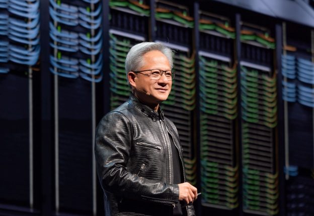
(Photo credit: NVIDIA)
Please note that this article cites information from Commercial Times, TechNews, Tom’s Hardware, and TSMC.