Popular Keywords
About TrendForce News
TrendForce News operates independently from our research team, curating key semiconductor and tech updates to support timely, informed decisions.
[News] Nikon Reportedly Aims Doubled Wafer Alignment Sales by FY27 as 3D Stacking, Wafer Bonding Rise
Shortly after announcing its plan to close the Yokohama Plant, Nikon seems to double down its efforts on advanced node related chipmaking tools. According to Nikkan Shimbun, the Japanese semiconductor equipment firm aims to double sales of its wafer alignment stations—which measure wafer distortion before photolithography—by FY2027 versus FY2024.
The report highlights Nikon’s “alignment station” as a key advantage, measuring wafer distortion to boost overlay precision for exposure tools. With 3D stacking and wafer bonding rising in NAND and logic chip production, Nikon is reportedly eyeing growth outside the EUV segment, where ASML currently dominates.
It is also worth noting that Nikon’s semiconductor lithography business faces a key hurdle, while among the top three foundries – TSMC, Intel and Samsung – only Intel is currently a customer, as per Nikkan. To broaden its footprint, Nikon aims to ramp up alignment station sales, with a new FY2026 model cutting measurement errors further and a successor already planned for FY2029, the report adds.
This is not the only try Nikon has made on advanced chipmaking tools. BITS&CHIPS reported in February that the company plans to launch a new ArF immersion lithography system in FY2028, designed for better compatibility with ASML products. Nikkan Kogyo Shimbun notes that Nikon is co-developing the system with semiconductor clients to support ASML photomasks, easing customer transitions, with next-generation models slated for post-2030.
Read more
- [News] Nikon Announces Yokohama Plant Closure as Precision Equipment Business Weakens
- [News] Nikon Unveils DSP-100 System for Panel-Level Packaging, Supporting 600mm Panels with 9x Throughput
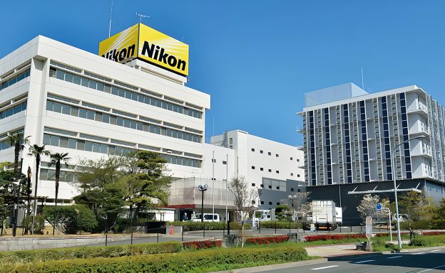
(Photo credit: Nikon)
Please note that this article cites information from Nikkan Shimbun and BITS&CHIPS.