Popular Keywords
About TrendForce News
TrendForce News operates independently from our research team, curating key semiconductor and tech updates to support timely, informed decisions.
[News] Three Semiconductor Makers Accelerate the Development of HBM & Advanced Packaging Equipment
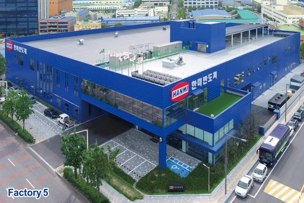
Hanmi Semiconductor Forms HBM4 Equipment R&D Team
Recently, Hanmi Semiconductor officially announced the establishment of a dedicated team focused on the development of HBM4-related equipment.
On May 14, the company launched the “TC Bonder 4,” specifically designed for HBM4 production. Chairman Kwak Dong-shin stated that with the relaxed height standards of HBM4, the new TC Bonder 4, featuring significantly improved production efficiency and precision, will support global customers in mass-producing HBM4 in the second half of this year.
As the sixth generation of high-bandwidth memory, HBM4 offers a 60% speed increase and 30% reduction in power consumption compared to HBM3E. It supports up to 16-layer stacking and 2,048 TSV (Through-Silicon Via) connections, greatly enhancing data transmission capabilities.
AMEC Fully Deploys in HBM and Advanced Packaging Fields
On June 9, AMEC disclosed on its investor interaction platform that it has made comprehensive deployments in the high-bandwidth memory (HBM) and advanced packaging fields.
According to the company’s secretary, AMEC’s product lines in advanced packaging — particularly those relevant to HBM processes — already cover etching, CVD, PVD, and wafer metrology and inspection equipment. Notably, AMEC has officially launched its CCP etching systems and core TSV deep silicon etching equipment.
In response to investor inquiries about dedicated HBM equipment development, AMEC emphasized that its advanced packaging equipment portfolio broadly covers key tools required for HBM processes. Specifically, in deep TSV etching technology, AMEC has achieved breakthroughs through in-house development and is now capable of supporting mass production needs, positioning the company to play a critical role in the HBM supply chain.
ACM Secures Approval for RMB 4.482 Billion Private Placement
On June 6, ACM Research (Shanghai) announced that its application for a private placement of no more than RMB 4.482 billion had been approved by the Shanghai Stock Exchange.
According to the previously disclosed proposal, the net proceeds will primarily fund three core projects: the R&D and process testing platform (approx. RMB 922 million), high-end semiconductor equipment iteration R&D (approx. RMB 2.255 billion), and working capital replenishment (approx. RMB 1.304 billion).
Additionally, the company recently revealed several new technologies closely tied to HBM and advanced packaging, including wet cleaning and electroplated copper (ECP) technologies.
ACM Shanghai’s proprietary megasonic cleaning technology and multifunctional integrated platform efficiently remove tiny particles and chemical residues from wafer surfaces, ensuring ultra-clean surfaces, which are critical for HBM stacking yield. The company is continuously upgrading its Ultra C series cleaning tools, such as optimizing cleaning for 3D structures and advanced nodes, and its Ultra C v series single-wafer vertical cleaners, all aimed at meeting the ultra-cleanliness and high-yield demands of HBM and other advanced packaging technologies.
Moreover, ACM’s ECP technology shows significant advantages in filling high aspect-ratio TSVs and forming RDLs (Redistribution Layers) and micro-bumps used in advanced packaging. The company is launching increasingly advanced electroplating systems, like its Ultra ECP GIII platform, designed for high-performance computing (HPC) and advanced packaging applications, offering exceptional capabilities for fine-pitch micro-bump and TSV filling — key requirements for advancing HBM technology.
(Photo credit: Hanmi Semiconductor)