


[News] Rapidus Scales Up Advanced Packaging, Targets 8-Reticle Interposers With 600mm Panels by 2030
Advanced packaging is taking on a bigger role as AI reshapes how semiconductor systems are designed and manufactured. Rapidus is responding with a roadmap centered on larger interposers and panel-level packaging. According to TechNews, Rozalia Beica, CTO of packaging at Rapidus Design Solutions, outlined the company’s strategy at the 2026 OCP APAC Summit, highlighting a broader industry shift from chip scaling toward system-level integration.
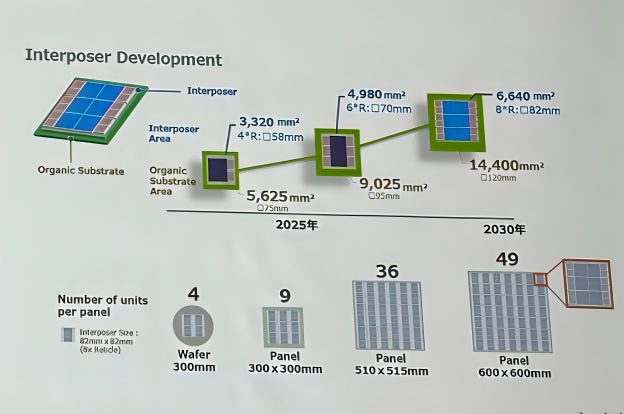
Rapidus is targeting eight-reticle-size interposers for high-performance chips by around 2030, according to ICVIEWS. Beica outlined a roadmap from four reticles at 3,320 mm² to six at 4,980 mm² and eventually eight at 6,640 mm². By 2030, the accompanying organic substrate is expected to reach 14,400 mm², setting the package-size target for Rapidus’ 600 × 600 mm panel-level advanced processor packaging.
For comparison, TSMC is moving even faster on interposer scaling, with its CoWoS roadmap advancing from 5.5-reticle size in 2026 to 9.5-reticle in 2027 and 14-reticle in 2028, according to EE Times. However, the two companies are pursuing different manufacturing approaches, with Rapidus betting on 600 × 600 mm panel-level processing for large-format interposers.
Rapidus is developing solutions for both 300 mm wafers and 600 mm panels, with the latter already demonstrated. Beica compared the output of an eight-reticle-size interposer across four formats: four units on a 300 mm wafer, nine on a 300 × 300 mm panel, 36 on a 510 × 515 mm panel, and 49 on a 600 × 600 mm panel, as noted by TechNews.
Rapidus Advances 600mm Panel-Level Packaging
Rapidus has already laid the groundwork for its 600mm packaging strategy. Under its FY2026 plan, the company is bringing its Rapidus Chiplet Solutions (RCS) pilot line into full-scale operation to verify 2.xD and 3D packaging processes, while advancing 600 × 600 mm panel-level packaging for high-density chiplet integration.
The company is also tapping Lam Research’s panel-level packaging technology. According to EE Times Japan, Rapidus is developing 2.xD packaging with RDL (redistribution layer) formed on 600mm-square glass carriers, with Lam Research’s Kallisto electroplating system playing a key role. Nikkei previously reported that Rapidus unveiled what it claims is the world’s first large-format glass interposer prototype in late 2025, with mass production targeted for 2028.
Rapidus Pushes Front-End and Back-End Integration
Beyond its panel-level packaging efforts, Rapidus is developing a new manufacturing model that Beica calls “Innovative Integration and Manufacturing” (IIM). TechNews notes that the model uses AI and sensor data to monitor wafer conditions in real time, predict defects, and feed insights back into design, enabling joint optimization of design and manufacturing. Beica said the facility will effectively be the world’s first fab to integrate front-end and back-end processes under one roof.
Rapidus also plans to work closely with customers on their design needs. According to TechNews, its advanced packaging portfolio will include flip-chip BGA, 2.5D silicon interposers, panel-level RDL organic interposers, solutions with or without bridges, and 3D stacking with hybrid bonding.
Looking toward 2030, Beica expects future systems to integrate sub-2nm logic, high-bandwidth memory, chiplets, optical interconnects, hybrid bonding, and panel-level packaging, TechNews notes.
Read more
- [News] Rapidus Reportedly Taps Lam Research Panel-Level Packaging System for 600mm Square Glass Interposer Push
- [News] Japan’s Rapidus Takes on TSMC With Aggressive 2nm Pricing, Reportedly Targeting up to ¥3.5M per Wafer
(Photo credit: TrendForce)


