


[News] Huawei Unveils New Semiconductor Principle – Tau (τ) Scaling Law
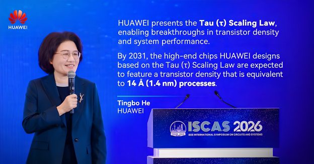
At the 2026 International Symposium on Circuits and Systems (ISCAS), held in Shanghai on Sunday, Huawei officially introduced the Tau (τ) Scaling Law during a keynote speech titled Exploration and Practice of New Semiconductor Pathways, delivered by He Tingbo, Huawei board member and president of the company’s semiconductor business department.
The announcement marks the first time a China-proposed semiconductor principle has been put forward as a framework intended to guide “evolution of both semiconductors and electronic systems.
Built on the new law, Huawei said it has designed and mass-produced 381 chips over the past six years. The company also plans to launch a new Kirin smartphone processor this autumn, which will fully adopt its LogicFolding architecture to deliver significant performance gains.
The Tau Scaling Law proposes replacing traditional “geometric scaling” with “time (τ) scaling”, aiming to systematically reduce time constants across semiconductor systems. Through innovations like LogicFolding architecture, the approach seeks to continuously compress signal propagation delays and increase transistor density, enabling sustained advances in semiconductors and electronic systems.
In recent years, Moore’s Law has faced mounting pressure from both physical limitations and diminishing economic returns. As the pace of transistor miniaturisation slows and the cost advantages of geometric scaling fade, the global semiconductor industry has increasingly grappled with how to move beyond conventional process pathways and establish a sustainable route for continued performance improvement amid surging computational demand.
The Tau Scaling Law introduces a multi-layer optimisation framework spanning devices, circuits, chips and system-level architectures. Huawei expects high-end chips developed under the new framework to achieve transistor densities equivalent to a process node of 1.4 nanometre by 2031.
(Photo credit: Huawei on X)


