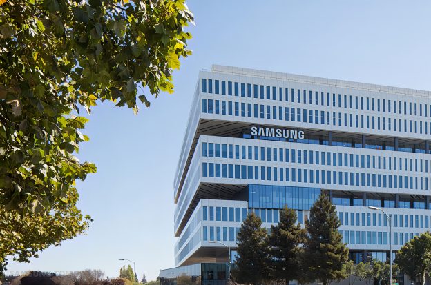
[News] Samsung Reportedly to Build a New Wafer Fab in the U.S.
As per a report by the Korea JoongAng Daily, mounting capacity constraints at TSMC have prompted major U.S. technology firms to queue for alternative foundry support. Against this backdrop of surging demand, Samsung Electronics is accelerating preparations to build a second wafer fabrication plant (Fab 2) at its semiconductor campus in Taylor, Texas. The project has now entered the preliminary stage of regulatory review and planning.
Recently, the Taylor City Council unanimously approved an amendment extending the city’s contract with HDR Engineering, Inc., enabling continued support for Samsung’s planned Fab 2 through development permitting and regulatory processes.
Under the agreement, HDR Engineering will undertake several critical responsibilities, including reviewing fab design plans, assisting Samsung in securing construction permits, managing permit issuance procedures, and ensuring compliance with building codes and regulations. Once the necessary permits are granted, construction of Fab 2 is expected to commence immediately.
Fab 2 is estimated to cover approximately 2.7 million square feet—matching the size of the currently under-construction Fab 1. However, Samsung’s ambitions extend well beyond these two facilities.
To support long-term expansion, Samsung has acquired a total of 1,268 acres in Taylor to establish a dedicated semiconductor cluster. The site is large enough to accommodate up to 10 advanced wafer fabs, providing substantial flexibility for future capacity growth.
Looking back, Samsung selected Taylor, Texas in November 2021 as the location for its second U.S. foundry hub and officially broke ground in 2022. Initially announced with an investment of USD 17 billion, the project has since expanded significantly, with total investment now reaching USD 37 billion. Notably, this includes USD 4.75 billion in subsidies from the U.S. federal government under the CHIPS and Science Act.
From a technology perspective, the Taylor campus will primarily focus on producing advanced chips for high-performance computing (HPC) and automotive applications, leveraging Samsung’s most advanced 2nm process technology.
Market sources indicate that Samsung has already secured orders from as many as 121 customers for the site. Future large-scale orders are widely expected to come from leading global tech firms such as Google, AMD, and ByteDance.
Meanwhile, Fab 1 at the Taylor campus is progressing steadily and is scheduled to begin mass production in 2027. This timeline aligns with a key partnership between Samsung and Tesla.
Under a USD 16.5 billion agreement, Samsung will manufacture Tesla’s next-generation AI5 and AI6 chips. While it remains unclear whether Tesla will expand the contract beyond AI6, CEO Elon Musk previously stated on the social platform X that AI5 is expected to enter mass production around mid-2027.
According to Taylor city officials, Samsung had already secured a temporary permit as of February 2026, covering approximately 88,000 square feet within Fab 1. This suggests that certain areas of the facility have entered early-stage operational preparation. Additionally, under agreements signed with the city, Samsung is committed to completing a total of 6 million square feet of facility space at the site.
From a competitive standpoint, data from TrendForce indicates that Samsung’s foundry business revenue rose 6.7% quarter-over-quarter in 4Q25 to USD 3.4 billion. Its global market share also increased from 6.8% to 7.1%, solidifying its position as the world’s second-largest foundry. With the advancement of Fab 2 and the rollout of its 2nm process, Samsung is aiming to strengthen its foothold in an increasingly competitive global semiconductor landscape.
(Photo credit: Samsung)


