[News] Chinese and U.S. Researchers Jointly Achieved Breakthrough in Novel Chip Materials

As per Xinhua News Agency, a research team led by Professor Zhang Shuchen of the University of Science and Technology of China (USTC), in collaboration with researchers from Purdue University in the United States and ShanghaiTech University, has made a remarkable advance in the field of novel semiconductor materials.
For the first time, the team has realized the controllable fabrication of in-plane, programmable, atomically flat “mosaic” heterojunctions within two-dimensional ionic soft-lattice materials, opening up a new pathway for the development of next-generation high-performance light-emitting and integrated devices. The research results were published in Nature on January 15.
Ionic soft-lattice semiconductors, represented by two-dimensional halide perovskites, feature flexible yet structurally unstable crystal lattices. Conventional fabrication techniques such as photolithography often involve aggressive processing steps that can damage these materials, making it difficult to achieve high-quality lateral heterointegration. How to achieve precise, controllable lateral heterojunctions with high-quality epitaxy in such materials has therefore remained a major scientific challenge in the field.
The research team reported that it has creatively proposed and developed a new approach based on guided “self-etching” driven by internal crystal stress. During growth, two-dimensional perovskite single crystals naturally accumulate internal stress. By carefully designing a mild ligand–solvent microenvironment, researchers were able to selectively activate and harness this internal stress, inducing controllable self-etching at designated locations within the single crystal and forming regular, square-shaped pore structures.
Later, a rapid epitaxial growth process was applied to precisely refilled different semiconductor materials into these predefined regions, ultimately enabling the construction of high-quality “mosaic” heterojunctions within a single crystal wafer. These heterostructures feature continuous lattices and atomically flat interfaces.
According to the researchers, this work represents the first demonstration of high-quality, designable lateral heterojunction fabrication in two-dimensional ionic material systems, overcoming the limitations of traditional processing techniques. By introducing a new paradigm for harnessing internal crystal stress and kinetics to achieve programmable evolution of functional structures within a single crystal, the study provides a powerful platform for investigating idealized interfacial physics and creates new avenues for the integration and device application of low-dimensional materials.
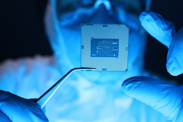
(Photo credit: FREEPIK)


