[News] Chinese Semiconductor Research Achieves Multiple Breakthroughs in Memory and IC Design

Recently, a number of Chinese universities and research institutions have achieved major progress in semiconductor-related fields. These advances span key areas such as memory, power semiconductor and IC design.
IME CAS Achieved Major Progress in High-Density 3D DRAM Research
A research team from the National Key Laboratory of Integrated Circuit Manufacturing Technology at the Institute of Microelectronics of Chinese Academy of Sciences (IME CAS), in collaboration with the Beijing Superstring Academy of Memory Technology(SAMT) and Shandong University, has proposed a novel dual-gate 4F² 2T0C memory cell architecture.
By adopting an in-situ metal self-oxidation process, the technology enables self-aligned integration of the read and write transistors within a 4F² memory cell. Combined with multi-level storage techniques, it can further increase storage density.
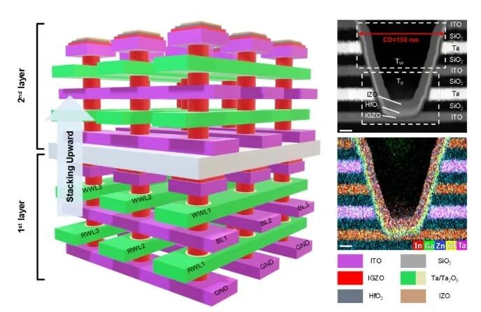
Figure 1. Schematic and SEM characterization of the 4F² dual-gate 2T0C memory array
(Credit: Institute of Microelectronics of Chinese Academy of Sciences)
Test results show that the vertical dual-gate transistor delivers excellent on-state current and subthreshold swing, along with strong reliability performance in 85 °C thermal stability tests, achieving −22.6 mV (NBTS) and 87.7 mV (PBTS). The transistor thus combines high performance with high stability. Based on this device, the 4F² 2T0C cell supports 4-bit multi-level storage, achieving a write time of 50 ns and data retention exceeding 300 s, demonstrating strong technological potential.
Nanjing University of Science and Technology Reported New Results in Power Semiconductor
Recently, a joint research team from the School of Microelectronics (School of Integrated Circuits) at Nanjing University of Science and Technology proposed a new switching-loss prediction method based on multilayer backpropagation artificial neural networks (ANNs).
The approach leverages regression relationships between static parameters of SiC MOSFETs—such as threshold voltage, leakage current and on-resistance—and switching losses. Without the need for complex physical modeling or parameter extraction, switching losses can be rapidly and accurately predicted using only measured data or static parameters from datasheets.
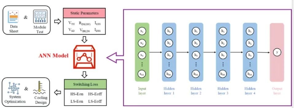
(Credit: Nanjing University of Science and Technology)
Experimental results on a 1200 V SiC MOSFET power module dataset show that the method achieves a minimum mean absolute percentage error (MAPE) of 1.13%, with a maximum error below 7.43%. The average prediction time per module is only 4.95 ms, outperforming benchmark methods. Moreover, when deployed on NVIDIA Jetson embedded platforms, the model shows no performance degradation, demonstrating practical applicability. The method provides a new solution for thermal design optimization and large-scale quality screening of power modules.
HKU, Wuhan University and CAS Jointly Made Major Progress in 4H/3C-SiC Composite Substrates and Devices
Recently, a team led by researcher Liu Xinyu from the High-Frequency and High-Voltage Center of IME CAS, in collaboration with the University of Hong Kong, Isabers Group, Wuhan University and the Institute of Physics CAS, successfully developed large-area 4H/3C-SiC single-crystal composite substrates, breaking the specific on-resistance limit of low-voltage (<600 V) 4H-SiC devices.
The team proposed an innovative heterogeneous integration scheme combining a “high-quality 4H-SiC thin film + low-resistance 3C-SiC substrate.” This approach preserves the high crystalline quality and high breakdown field strength of 4H-SiC while fully leveraging the low resistivity of 3C-SiC, effectively resolving a long-standing trade-off that has constrained device development. The resistivity of the heterogeneously integrated substrate is reduced to 0.39 mΩ·cm—45 times lower than that of conventional 4H-SiC substrates—offering a new pathway for performance leaps in low-voltage SiC power devices.
SUSTC Research Team Achieved Key Results in High-Speed IC Design
Recently, the team led by Pan Quan at the School of Engineering and National Demonstration Microelectronics College, Southern University of Science and Technology (SUSTC), achieved further breakthroughs in high-speed communication and optoelectronic IC design.
1. A 56 Gbaud, 7.3-Vppd Linear Modulator Transmitter Based on AMUX Inherent Feed-Forward Equalization and a Breakdown-Voltage Tripler
The work proposes a half-rate linear transmitter monolithically integrating a 2:1 analog multiplexer (AMUX) and a linear driver for optical modulators. By exploiting the timing relationship between the clock and half-rate data streams, the AMUX inherently implements a feed-forward equalizer (FFE), which can be reconfigured into two-tap or three-tap modes by adjusting clock delay.
To further enhance output voltage swing and linearity, the authors propose a novel “breakdown-voltage (BV) tripler” topology for the linear driver. By stacking three heterojunction bipolar transistors (HBTs) and using the amplified input signal to bias the bases of the top two HBTs, the driver achieves three times the output swing of conventional cascode topologies while maintaining good reliability.
Fabricated in a 130-nm SiGe BiCMOS process, the proposed linear driver achieves 17.1 dB DC gain, a 39.1 GHz 6-dB bandwidth, and 1.6% total harmonic distortion (THD) at 6-Vppd, 1-GHz sine-wave output. The complete transmitter (AMUX + driver) delivers a maximum output swing of 7.3 Vppd at 56-Gb/s NRZ operation, and when the inherent FFE is enabled, supports up to 112-Gb/s PAM-4 transmission at a 4.2-Vppd swing—representing a key breakthrough for next-generation high-speed optical interconnects.
2. A 112 Gb/s Single-Ended Receiver Front-End Based on Multi-Order Crosstalk Cancellation and Signal Multiplexing
The paper also presents a 112-Gb/s single-ended PAM-4 receiver front-end for backplane links, based on multi-order crosstalk cancellation and signal reuse techniques. An Nth-order far-end crosstalk (FEXT) model is introduced to accurately capture real FEXT behavior at higher frequencies. Based on this model, a novel multi-order crosstalk cancellation and signal reuse (M-XTCR) technique is proposed to minimize residual crosstalk while enhancing reuse of high-frequency signal components.
Beyond more thoroughly suppressing residual crosstalk, the approach converts extracted crosstalk energy into active enhancement of useful high-frequency signal components, improving signal quality while mitigating interference.
Fabricated in a 28-nm CMOS process, the receiver front-end adopts a second-order XTCR topology and is validated over a 4-inch channel with a signal-to-crosstalk ratio of 33 dB. Measurement results show that, compared with conventional first-order XTCR, the second-order XTCR improves horizontal and vertical eye openings by 21% and 34%, respectively, at 56-Gb/s NRZ, and by 24% and 18% at 112-Gb/s PAM-4. The design achieves an energy efficiency of 0.34 pJ/b, outperforming the state of the art and laying a solid foundation for practical high-density single-ended interconnect systems.
(Photo credit: FREEPIK)


