


[News] HKC Announced Investment in Advanced Semiconductor Packaging and Testing
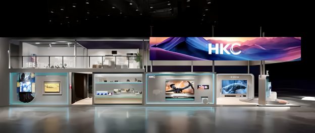
On July 17, HKC announced that it had signed a cooperation agreement with the Administrative Committee of the Shaoxing Area of the Hangzhou–Shaoxing Airport Economic Integration Demonstration Zone to develop an advanced semiconductor packaging and testing project.
The company plans to invest CNY 4 billion to establish a wholly owned subsidiary, Zhejiang Huixin Advanced Semiconductor Co., Ltd., which will serve as the project’s operating entity.
The project will be carried out in two phases. Phase I will build a 12-inch advanced packaging and testing line for heterogeneous chip integration, targeting a production capacity of 20 million units per month upon full ramp-up. Construction is expected to be completed within three years, with the final scope subject to the approved feasibility study and project application.
Phase II will be launched at an appropriate time based on the progress of the first phase. Its investment scale, timeline, and implementation plan will be determined through further negotiations and formal investment agreements between the two parties.
HKC stated that the new subsidiary will have a registered capital of CNY 4 billion, funded entirely through the company’s own capital. The investment is expected to be deployed in stages over the next two to three years in line with the project’s construction schedule, which is anticipated to have a certain impact on the company’s cash flow.
Against the backdrop of a restructuring global semiconductor supply chain and steadily rising demand for chip packaging and testing services in China, HKC said the investment marks its entry into the advanced packaging and testing segment. The move represents a strategic expansion into a higher value-added segment of the semiconductor value chain and is expected to cultivate a new engine of business growth.
(Photo credit: HKC)


