[News] Korea’s POSTECH Develops Tech for Stable 10+ Layer Chip Stacking, Achieving 4× the Density of 12-Hi HBM
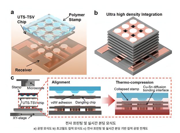
South Korea’s Pohang University of Science and Technology (POSTECH) has developed a new chip stacking technology that can stably stack more than 10 layers of ultra-thin semiconductor chips, each just one-fifth the thickness of a human hair. According to ETNews, a research team led by Professor Kim Seok developed a process that integrates chip transfer and metal bonding into a single step. The technology achieved an integration density approximately four times higher than that of conventional 12-layer HBM, allowing significantly more chips to be stacked within the same package height. The study was published online in the international multidisciplinary engineering journal Results in Engineering.
HBM is built by vertically stacking multiple memory chips. However, as chips become thinner—typically below several tens of micrometers—they become increasingly susceptible to bending and cracking, a challenge that grows more severe as additional layers are stacked, the report notes.
To overcome this challenge, the researchers combined two technologies into a single process: transfer printing, which precisely positions chips, and in-situ bonding, which simultaneously forms metal interconnections during transfer. According to the report, the process completes chip transfer, bonding, and electrical connection in a single step.
New Process Targets AI Chips, Chiplets, and Micro LEDs
The report says the new process enabled the stable stacking of more than 10 ultra-thin chips at temperatures below 180°C and pressures below 20 kPa. Even after repeated stacking, interlayer alignment errors remained minimal while chip warpage was significantly reduced. To validate the process, the team fabricated ultra-thin silicon chips approximately 14 μm thick, each incorporating vertical electrical interconnects and lateral wiring structures optimized for multi-layer stacking.
The technology could enable significantly more chips to be integrated within the same package footprint, substantially improving AI semiconductor performance, the report says. It could also be applied to chiplet packaging, which integrates multiple functional chips into a single package, as well as next-generation Micro LED displays.
Read more
- [News] Intel Patent Reveals XBM Matching HBM4 Footprint Without Interposers; Commercialization Seen After 2030
- [News] Samsung, SK hynix Reportedly Reconsider Hybrid Bonding Timeline; 16-High HBM4E May Be Earliest Adoption
(Photo credit: POSTECH)