Popular Keywords
About TrendForce News
TrendForce News operates independently from our research team, curating key semiconductor and tech updates to support timely, informed decisions.
[News] Chinese Scientists Advances Lithium Tantalate–Silicon Nitride Heterogeneous Integrated Photonic Chips

Recently, a research team led by Prof. Ouxin at the Shanghai Institute of Microsystem and Information Technology under the Chinese Academy of Sciences, in collaboration with the team of Prof. Tobias J. Kippenberg at École Polytechnique Fédérale de Lausanne and Prof. Christian Koos at Karlsruhe Institute of Technology, has reported progress in wafer-scale heterogeneous integration of thin-film lithium tantalate (LiTaO₃, LT) and silicon nitride (Si₃N₄) photonic chips.
The team developed a new optoelectronic platform that combines ultra-low optical loss with linear electro-optic (Pockels) modulation capability.
Based on this platform, the researchers demonstrated highly efficient, high-speed electro-optic modulation. The device achieved a modulation efficiency of 4.08 V·cm and an electro-optic response 3 dB bandwidth of approximately 100 GHz. The team further conducted high-speed communication demonstrations: the net data transmission rate reached 333 Gbit/s using intensity modulation and direct detection (IMDD), and 581 Gbit/s under coherent IQ modulation.
This work effectively fills the long-standing gap of high-speed electro-optic modulation capability in existing silicon-nitride photonic platforms, while also providing a scalable fabrication route for on-chip optical systems targeting high-speed interconnects, RF photonics, and analog signal processing.
Silicon-nitride photonic chips offer several advantages, including ultra-low optical propagation loss, strong optical nonlinearity, high power tolerance, and compatibility with CMOS processes. As a result, they have become an important platform for on-chip nonlinear optics, efficient frequency conversion, and traveling-wave optical parametric amplification. However, due to intrinsic material limitations, silicon nitride itself does not exhibit the Pockels electro-optic effect. Consequently, current silicon-nitride-based modulators typically rely on thermo-optic or acousto-optic effects, which can encounter bottlenecks in both bandwidth and modulation efficiency.
In response to the growing demand for high-efficiency, high-speed, and broadband modulation in applications such as optical communications and optical computing, researchers increasingly rely on thin-film ferroelectric materials to build corresponding on-chip optical devices. At present, mainstream electro-optic platforms include thin-film lithium niobate (TFLN) and thin-film lithium tantalate (TFLT).
Historically, TFLN has been the more common choice, but TFLT has attracted increasing attention in recent years. While maintaining comparable electro-optic coefficients, thin-film lithium tantalate offers advantages in high-power device stability, birefringence characteristics, optical damage threshold, and photorefractive resistance. Moreover, its industrial deployment in 5G/6G RF filters has helped establish a more complete supply chain for optical-grade substrates, further enhancing its engineering appeal.
Against this backdrop, how to integrate the low-loss advantages of silicon-nitride waveguides with the high-speed electro-optic properties of thin-film lithium tantalate—while achieving wafer-scale, repeatable, and high-volume manufacturing—has become a major research focus.
Leveraging a silicon-nitride photonic Damascene fabrication process and wafer-bonding technology developed by the research team, the study successfully realized a 4-inch LT-on-Si₃N₄ heterogeneous wafer. As shown in Figure 1b, across nine primary write fields defined by deep-ultraviolet (DUV) lithography, the transferred lithium tantalate thin films achieved a nearly 100% integrity rate.
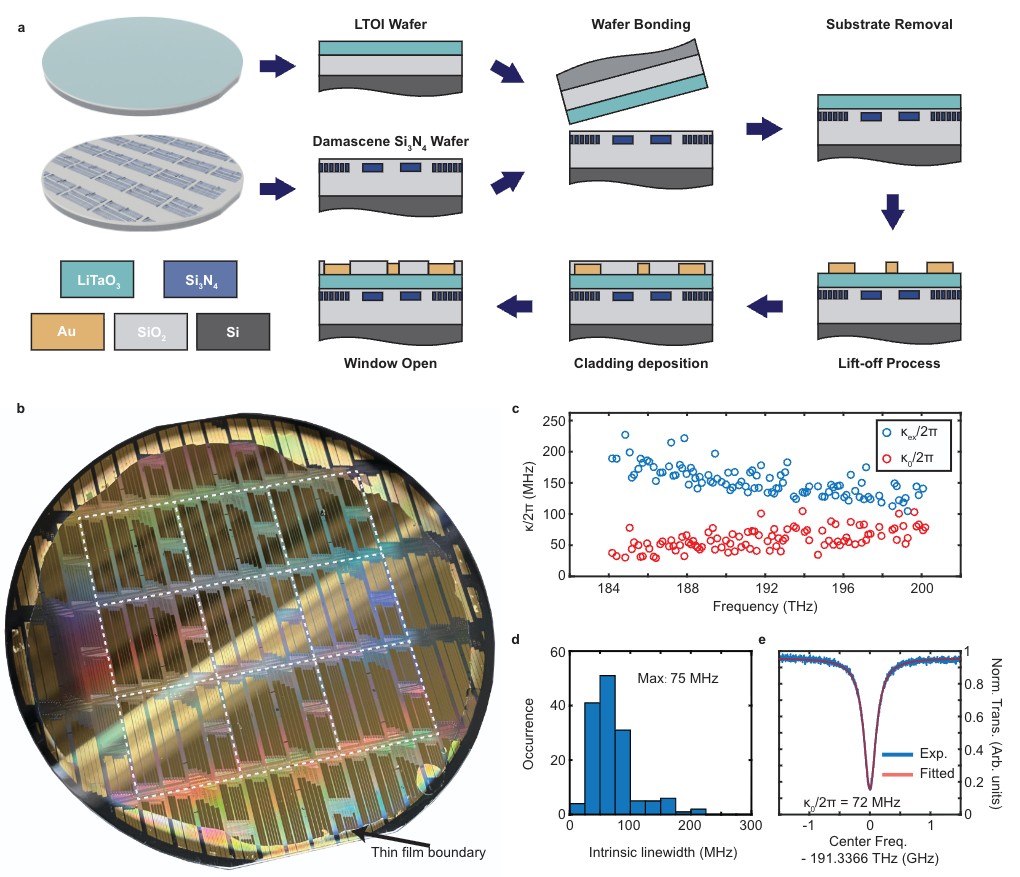
Figure 1. Wafer-scale fabrication process and optical loss characterization of Si₃N₄–LiTaO₃ structures
(Credit: Shanghai Institute of Microsystem and Information Technology)
Characterization using micro-ring resonators showed that the optical loss of the heterogeneous hybrid waveguide is approximately 14.2 dB/m—significantly better than comparable integration approaches.
The electro-optic modulator in this work adopts a Mach–Zehnder modulator (MZM) composed of thin-film lithium tantalate and silicon-nitride waveguides (Figure 2a). SEM observations of the heterogeneous waveguide cross-section, combined with finite-element simulations, indicate that approximately 48% of the optical mode energy is confined within the LT thin film, suggesting strong optical confinement and efficient overlap between the optical and electric fields.
Device measurements show a half-wave voltage of 6 V. The electro-optic response S21 curve exhibits excellent broadband flatness, with a 3 dB bandwidth approaching 100 GHz, while the return loss remains below –15 dB. These results confirm excellent velocity matching and impedance matching in the device.
Another highlight of the device is its DC bias stability. In system-level applications such as multi-channel signal transmission and optical computing, DC bias drift can directly cause fluctuations in output power, increasing control overhead and affecting long-term system stability.
With photonic chip packaging employed to suppress coupling drift, the researchers monitored the output intensity of the modulator at the quadrature operating point. The results show that power drift remained below 0.5 dB over one hour (Figure 2e). This stability benefits from the unetched lithium tantalate thin film within the heterogeneous integrated waveguide structure, which helps mitigate photorefractive effects introduced during etching and thereby enhances device stability.
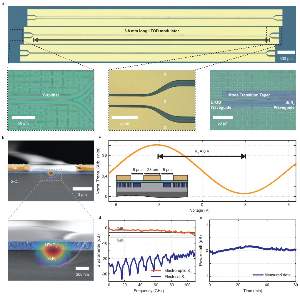
Figure 2. Heterogeneously integrated LT-on-Si₃N₄ electro-optic modulator
(Credit: Shanghai Institute of Microsystem and Information Technology)
In high-speed transmission experiments, the team tested the intensity modulator using PAM4 signaling at symbol rates ranging from 144 to 200 GBd. Achievable net data rates were evaluated based on GMI/NGMI metrics, with the highest net transmission rate reaching 333 Gbit/s at 192 GBd PAM4.
Furthermore, the heterogeneous platform also supports coherent IQ modulation. The coherent optical modulator consists of two MZMs, with a thermo-optic phase shifter providing a long-term stable 90-degree phase difference. Using two modulation channels, the researchers demonstrated transmission of formats such as QPSK and 16QAM, ultimately achieving a maximum net transmission rate of 581 Gbit/s.
These results set a new record for the highest signal transmission rate reported on similar integrated photonic platforms.
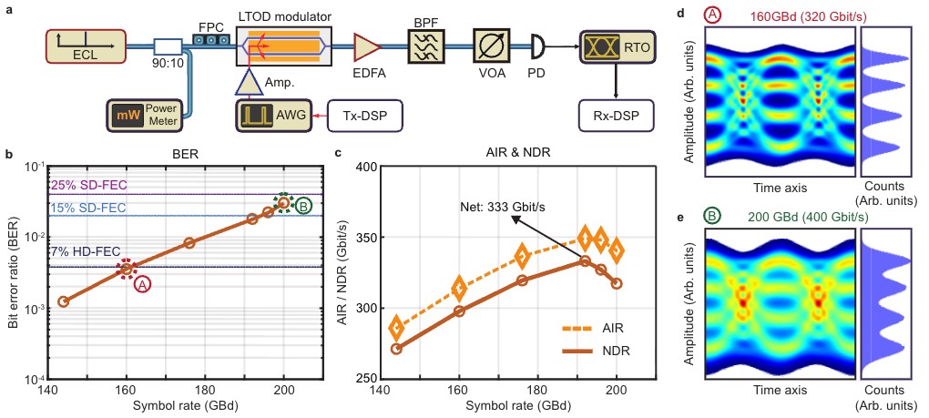
Figure 3. IMDD (PAM4-encoded) intensity-modulated signal transmission experiment
(Credit: Shanghai Institute of Microsystem and Information Technology)
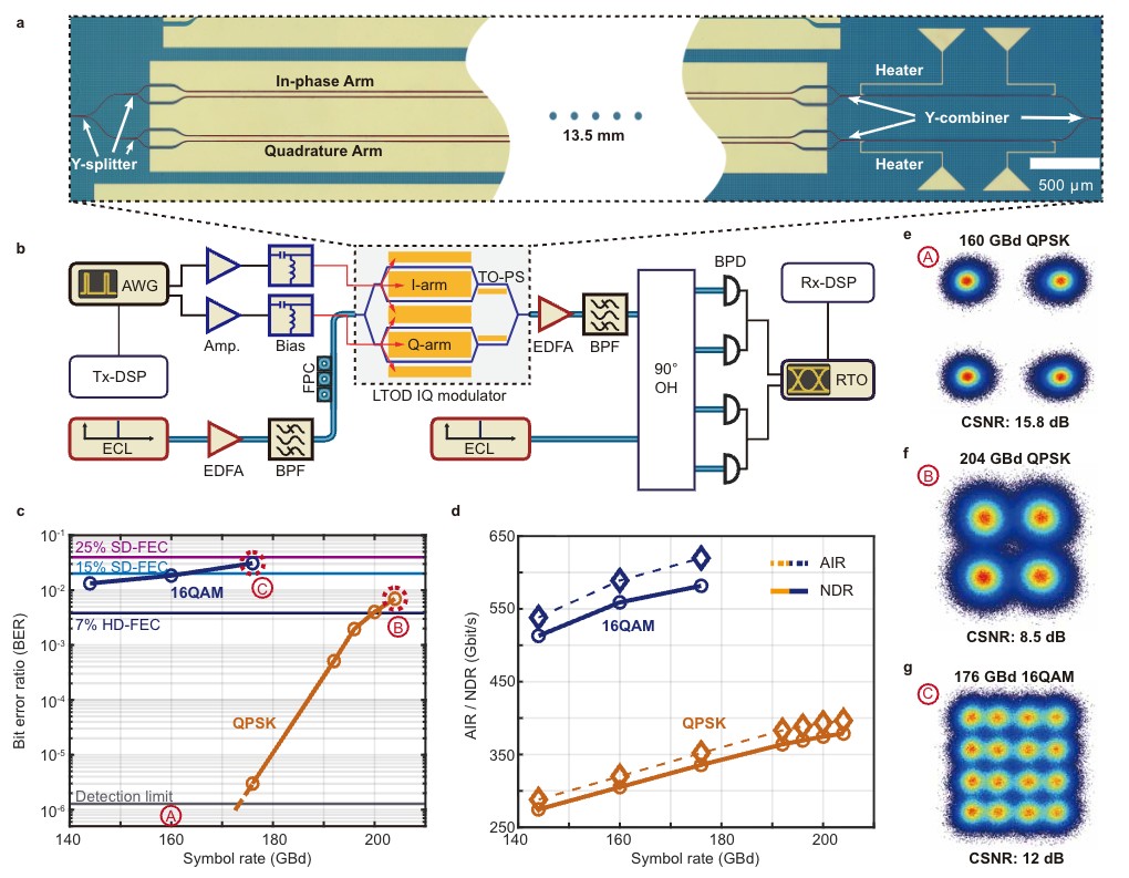
Figure 4. Coherent IQ (QPSK/16QAM-encoded) modulation signal transmission experiment
(Credit: Shanghai Institute of Microsystem and Information Technology)
(Photo credit: FREEPIK)