Popular Keywords
About TrendForce News
TrendForce News operates independently from our research team, curating key semiconductor and tech updates to support timely, informed decisions.
[News] HBM Etching Equipment Said to Enter a Super Cycle
At a time when the memory industry is in the midst of a boom deeply driven by artificial intelligence (AI), major memory makers are unanimously shifting their strategic focus toward AI-oriented storage solutions featuring high bandwidth, large capacity, and low power consumption. As demand for high-bandwidth memory (HBM) continues to surge, some vendors’ HBM capacity for 2026 have already all reserved, which is set to benefit suppliers of HBM-related equipment.
As HBM adopts a multilayer stacked DRAM architecture, the number of layers continues to increase in line with performance requirements. This makes inter-chip interconnect processes more complex and significantly increases the number of processing steps required.
Aside from international equipment giants, China’s equipment suppliers are also actively positioning themselves in the HBM equipment space, covering multiple segments such as etching, deposition, bonding, and inspection.
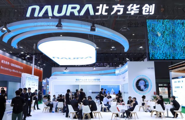
NAURA can provide a range of core tools for HBM chip manufacturing, including deep silicon etching, thin-film deposition, thermal processing, wet cleaning, and electroplating equipment.
Maxwell stated that its high-selectivity etching tools and hybrid bonding equipment can be applied to DRAM (HBM) processes. The company’s etching and thin-film deposition tools have already been widely used in the manufacturing of memory and logic chips.
U-Precision offers CMP tools, thinning equipment, dicing tools, and edge-polishing equipment as key core tools for chip stacking and advanced packaging processes such as HBM and CoWoS, which have already seen broad adoption among multiple leading customers.
(Photo credit: NAURA)