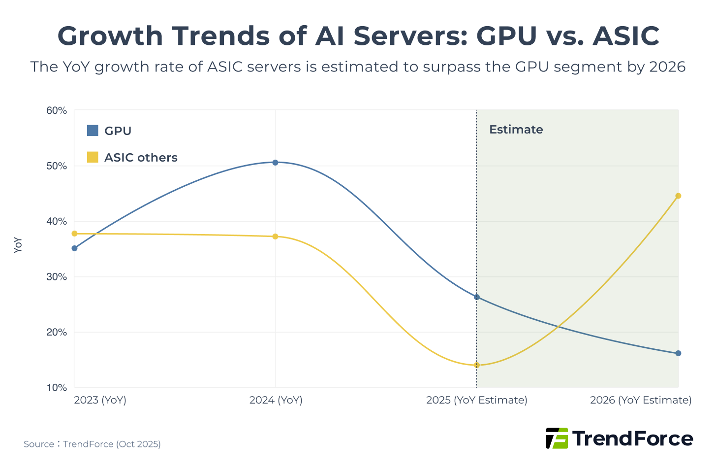
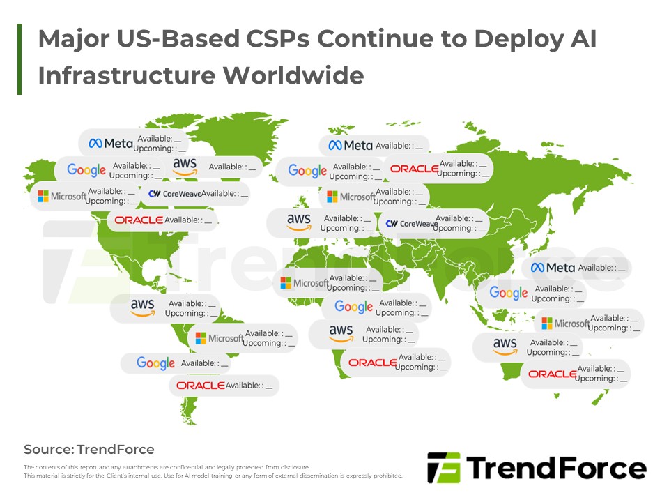
The AI accelerator market in 2026 is at a critical turning point. According to TrendForce data, based on growth rates in total AI server shipments (AI server shipments), In 2026, cloud service providers’ (CSPs) in-house ASICs are expected to grow by 44.6%, significantly surpassing GPUs at 16.1%.
Figure 1
However, this does not mean NVIDIA’s dominance will collapse overnight. Instead, the battle is shifting from a straightforward GPU performance race to a broader, more complex contest involving interconnects and the software ecosystem. NVIDIA’s golden era of “scale-up” leadership is entering a platform phase shaped by multiple forces.
Facing strong cost and efficiency pressure from the ASIC camp, NVIDIA’s response now goes beyond single-chip performance gains. Its recent moves, from technology roadmaps to product architecture, reveal a deliberate strategic shift.
- NVIDIA Launches NVLink Fusion:
Announcing NVLink technology is now open for customers to integrate into their own ASICs. This move aims to break its closed ecosystem and extend its strategic edge from hardware to the software layer of high-speed interconnects. - NVIDIA Introduces Rubin CPX/VR200 NVL144 CPX:
Designed for LLM inference, this new architecture adopts a novel rack concept and uses PCIe 6 interconnects between Rubin CPX chips. By separating the Prefill and Decode stages, it positions NVIDIA to capture a lower-tier but fast-growing inference market. - NVIDIA Collaborates with Intel:
The partnership expands NVLink usage to x86 CPUs. This enhances NVIDIA’s influence in server interconnects and broadens its ecosystem reach.
NVIDIA’s Business Strategy and Market Adaptation
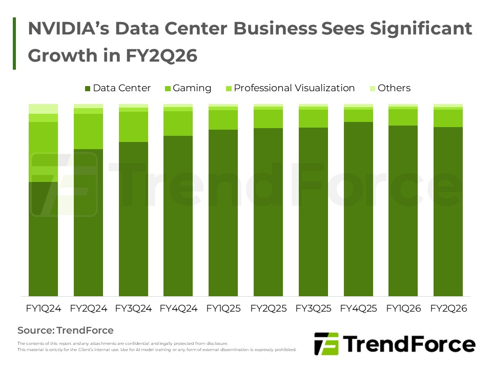
NVIDIA’s data center revenue accounted for nearly 88% in FY2Q26. GB Rack demand is expected to surge in 2H25, driven by Oracle, while H20 faces policy-related uncertainty in China. Get Trend Intelligence
The AI Data Center Interconnect Battle
Integration across multiple compute nodes has become a key driver of AI performance. Both NVIDIA, the current AI leader, and the ASIC camp led by Broadcom recognize that data center interconnects are essential for large-scale AI scaling, cross-node collaboration, and supercomputing power. Once a supporting component, interconnects are now a decisive factor, which is why both camps are actively advancing these technologies.
In AI infrastructure, interconnect networks can be categorized into three layers based on bandwidth, latency, node count, and transmission distance requirements:
- Scale-Up: vertical expansion within a single system (e.g., one rack or one SuperPOD)
- Scale-Out: horizontal expansion across multiple systems (e.g., around 4–16 SuperPODs forming a cluster)
- Scale-Across: expansion across data centers
Figure 2
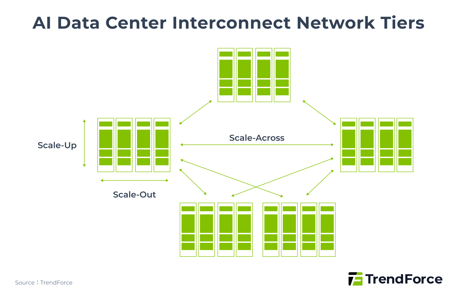
Table 1. Comparison of Scale-Up, Scale-Out, and Scale-Across in AI Data Centers
| Level | Scale-Up | Scale-Out | Scale-Across |
|---|---|---|---|
| Definition | Vertical expansion of a single system (Rack / SuperPOD) | Horizontal expansion across multiple systems (Cluster) | Expansion across data centers |
| Existing Protocols | NVLink, UALink, SUE, UB | InfiniBand, Ethernet, UE | Ethernet |
| XPU Bandwidth | ~ 8 Tbps | 400 / 800 Gbps | ~ 100 Gbps (E) |
| Latency Requirement | <1 μs | <10 ms | <20 ms (E) |
| Node Count | <10k | 10-100k | 1-10M |
| Transmission Distance | <500 m | 500 m - 10 km | <40 km |
| Topology | Clos, 3D Torus, Dragonfly+ | Clos, Dragonfly+ | Clos, Dragonfly+ |
| Hardware Technology | Rack-level, currently mostly copper, gradually moving to optical | Optical | Optical |
Note: (E) indicates Estimated.
(Source: TrendForce)
Impact of Network Topology and Structural Changes on Switch IC Demand
In network architectures, the pattern connecting compute nodes is referred to as the topology. Topology can generally be categorized as Hierarchical Topology, Direct-Connect Topology, or Hybrid Topology. Common network topology include Clos, Torus, Fully Mesh, and Dragonfly+, which combines Clos and Dragonfly.
Table 2. Major Network Topology Categories:
| Connection Type | Hierarchical | Direct-Connect | Hybrid |
|---|---|---|---|
| Definition | Uses a multi-layer structure | Nodes are directly connected | Combines hierarchical and direct-connect approaches |
| Examples | Clos | Torus, Full-Mesh, Dragonfly | Dragonfly+ |
| Illustration | 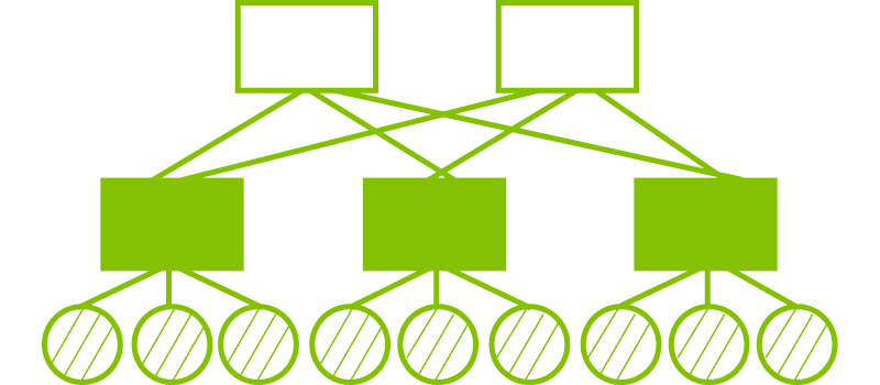 |
 |
 |
(Source: TrendForce)
The performance of a network topology can be evaluated using six key metrics:
- Performance
- Flexibility
- Modularity
- Divisibility
- Cost-effectiveness
- Symmetry
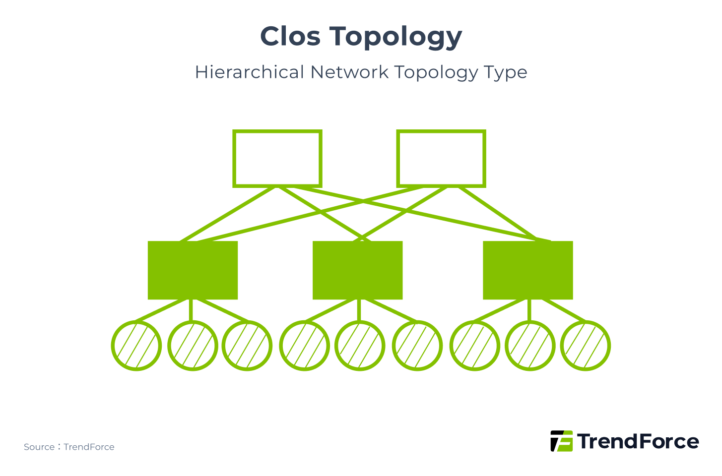
Among them, Clos (Figure 3), which belongs to the hierarchical topology category, is the most mature technology and performs well across all six metrics. Originally developed over fifty years ago for non-blocking telephone networks, the 2-Tier Clos (Leaf-Spine) architecture is now widely used in data centers. It supports multiple protocols and chips, including interconnects between Nvidia SuperPODs. Its main drawback is that its scalability is not as high as that of direct-connect topology.
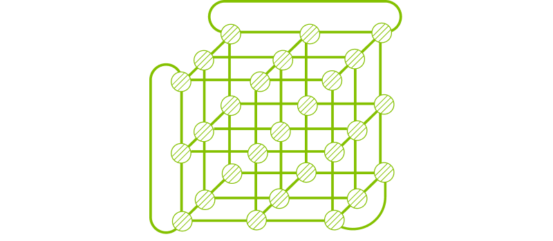
Figure 3
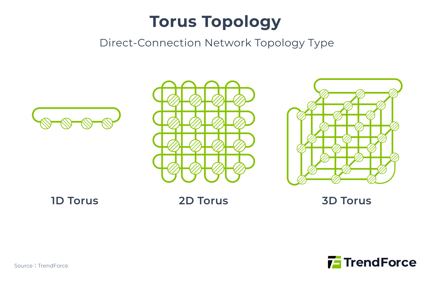
For direct-connect topology, Torus (Figure 4) offers excellent symmetry, modularity, cost efficiency, and flexibility. Since it does not require switches, the overall cost is less than 20% of a Clos-based network. Google’s current Inter-Chip Interconnect (ICI) network uses a 3D Torus architecture. However, Torus Topology are difficult to partition. When scaling up, using only a portion of the topology can lead to a significant drop in performance. For example, a single GPU with a total bandwidth of 7,200 Gbps may be directly connected to seven other GPUs. In this case, the bandwidth per link drops to 1,028 Gbps.
Figure 4
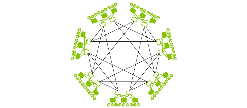
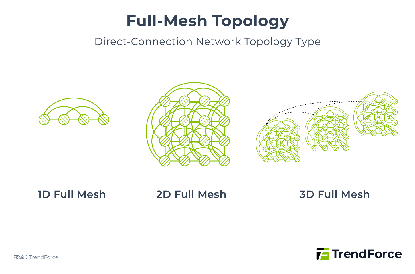
Full-Mesh (Figure 5) maintains a constant network diameter as the system scales, giving it performance advantages over Torus. However, it still suffers from partitioning difficulties and limited flexibility. In practice, Tesla’s TTP (Tesla Transport Protocol) employs a 2D Full-Mesh architecture.
Figure 5
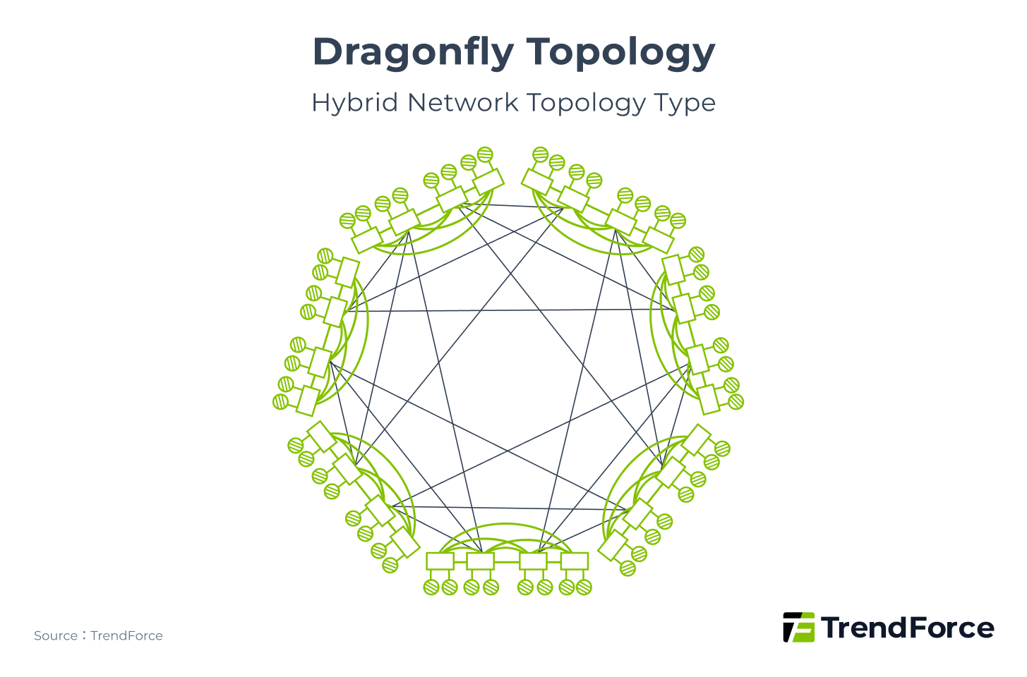
Dragonfly (Figure 6) connects multiple switches directly to improve scalability, offering better cost efficiency when scaling compared with Clos. However, its performance on a local scale is lower than Clos.
Figure 6
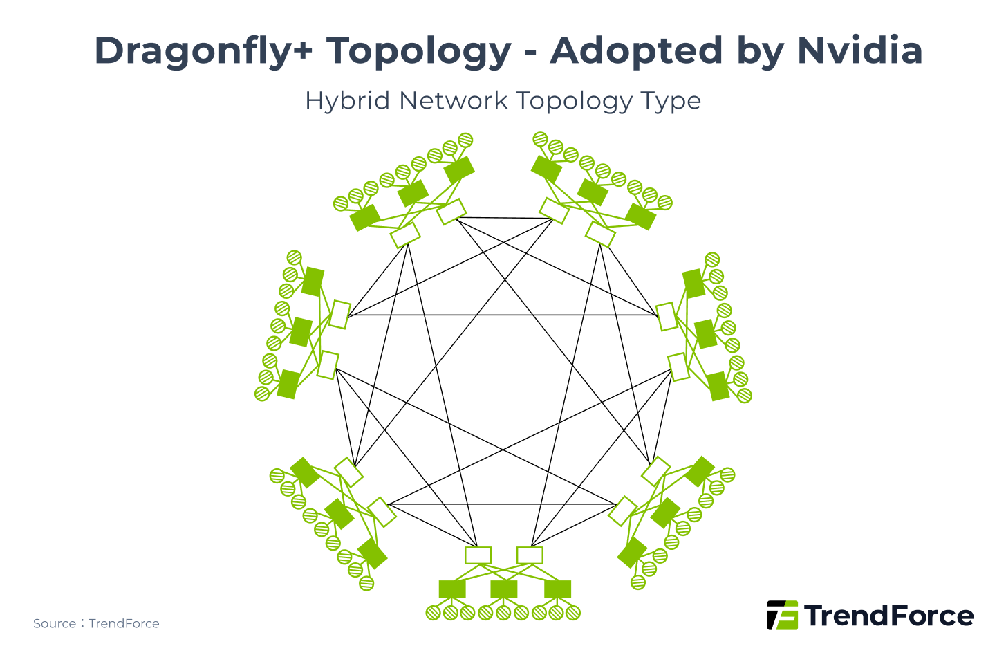
Hybrid Topology, which combine the advantages of hierarchical and direct-connect designs, have emerged to address both performance and scalability needs. NVIDIA’s Dragonfly+ (Figure 7) is a hybrid of Dragonfly and Clos. Within each switch group, it uses a 2-Tier Clos structure to enhance intra-group communication, ensuring that the interconnect bandwidth between GPU pairs remains unaffected by the number of GPUs. Between groups, it adopts a 1D Full-Mesh Dragonfly structure to improve scalability.
Figure 7
Are CSP Network Architectures Shifting Toward Hybrid Topology?
In the past, CSPs primarily adopted Scale-Up networks based on Torus or Mesh Topology that didn’t require switches. But as the number of XPUs connected to SuperPODs grows, CSPs aim to improve performance, scalability, and cost efficiency. To meet these goals, they are expected to gradually adopt Hybrid Topology that incorporate switches. This transition will, in turn, increase demand for Switch ICs.
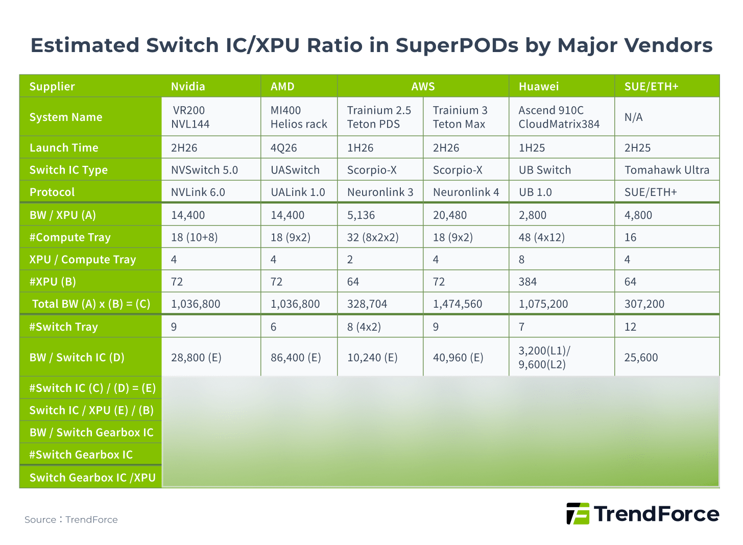
For example, AWS used a 3D Torus-based NeuronLink 3 in Trainium 2, but its upcoming Trainium 2.5 Teton PDS in 4Q25 will adopt a hybrid topology with Switch ICs, using customized chips from Astera Labs based on Scorpio-X.
Figure 8
Scale-Up Competition: NVIDIA’s Moat and Challengers
NVIDIA has established a strong leading position in the Scale-Up market with its NVLink technology. Its technology roadmap is clear: from NVLink 1.0 in 2014 to NVLink 5.0 in 2024, the bidirectional total bandwidth per GPU has jumped from 160 Gbps to 1,800 Gbps.
NVIDIA’s NVSwitch technology has evolved in parallel, enabling full interconnects for 16 GPUs initially and high-speed connections for 576 GPUs in NVL576 racks, keeping NVIDIA about a year ahead of competitors in technical specifications.
Notably, NVIDIA’s strategy is shifting from pure technical leadership to a more comprehensive ecosystem defense:
- Steady advancement in technical specs: Since NVLink 1.0 in 2014, NVIDIA has released new versions roughly every two years, continuously increasing per-GPU bandwidth and node count.
- Innovation in modulation technology: By moving from NRZ to PAM4, NVIDIA doubled transmission rates, reflecting sustained investment in underlying physical technologies.
- Diversified product architecture: Beyond the traditional DGX series, products such as GB200 NVL72 and VR200 NVL144 CPX provide more targeted and versatile rack solutions.
Table 3. NVLink Technology Evolution
| Launch | 2014 | 2017 | 2018 | 2020 | 2022 | 2024 | 2025 | 2026 | 2027 |
|---|---|---|---|---|---|---|---|---|---|
| GPU Type | P100 | V100 | A100 | GH100 | GH100 | GB200 | GB300 | VR200 | VR300 |
| DGX Name | DGX-1 | DGX-1 | DGX-2 | DGX A100 |
DGX H100
NVL32
|
NVL72 | NVL144 | NVL144 | NVL576 |
| NVLink | 1.0 | 2.0 | 3.0 | 4.0 | 5.0 | 6.0 | 7.0 | ||
| GPU per DGX | 8 | 8 | 16 | 8 |
8
32
|
72 | 72 | 144 | |
| NVSwitch | N/A | 1.0 | 2.0 | 3.0 | 4.0 | 5.0 | 6.0 | ||
| Lane per Port | 8 | 4 | 2 | 2 | 4 (E) | 4 (E) | |||
| BW/Lane | 20 Gbps | 25 Gbps | 50 Gbps | 100 Gbps | 200 Gbps | 200 Gbps (E) | 400 Gbps (E) | ||
| Modulation | NRZ | NRZ | NRZ | PAM4 | PAM4 | PAM4/PAM6 (E) | |||
| Structure | Cube Mesh | All-to-All | |||||||
Note: (E) indicates Estimated.
(Source: TrendForce)
However, this moat is not invincible. Major CSPs and chip vendors are actively developing their own Scale-Up technologies to reduce reliance on NVIDIA. AMD’s UALink, Broadcom’s SUE, and proprietary solutions from AWS and Google all aim to offer alternative architectures, either open or proprietary.
NVIDIA NVLink Fusion Opens New Ecosystem
NVIDIA’s NVLink Fusion strategy represents a key move in its competition with the ASIC camp. By opening the NVLink interface as an I/O IP, NVIDIA allows customers to integrate it into their own ASICs or CPUs. This not only gives customers access to NVLink’s high-speed connectivity but also effectively locks them into NVIDIA’s broader software ecosystem.
It’s a clever “give a little to gain more” approach, NVIDIA cedes part of the hardware market in exchange for deeper control over software and the ecosystem. Fujitsu and Qualcomm have already integrated NVLink Fusion into their CPU designs, demonstrating the effectiveness of this strategy.
China Battlefield: The Rise of Domestic Scale-Up Leaders
In the AI computing race, China has developed a competitive landscape largely independent of NVIDIA’s ecosystem. In addition to CSPs developing their own ASICs, domestic tech giants, especially Huawei, are building their own ecosystems in the Scale-Up space, directly challenging NVIDIA’s market dominance.
Currently, the main self-developed Scale-Up technology standards in China include:
- Huawei’s Unified Bus (UB): A leading closed solution that is gradually moving toward openness.
- Alibaba-led ALS (Alink System): An open alliance jointly promoted by Alibaba Cloud and AMD.
- Tencent-led ETH-X: An open standard focused on optimizing Ethernet performance.
2025 Global and China AI Data Centers: Deployment and Outlook
U.S. CSPs scale globally and invest more at home, while Chinese CSPs expand with self-developed chips, but both prioritize energy stability going forward. Get Trend Intelligence
Huawei’s UB Technical Strength and Market Ambition
Huawei’s UB protocol is the most mature and largest-scale Scale-Up solution in the Chinese market. In 2025, Huawei launched the Atlas 900 A3 SuperPOD based on UB 1.0, featuring scale and interconnect efficiency.
The system provides high-speed interconnects among 384 Ascend 910C NPUs, each with up to 400 Gbps bandwidth. Notably, its CloudMatrix384 architecture adopts a 2D-Full Mesh hybrid design. This enables high-density interconnects at both the single-board and single-rack levels, rather than merely stacking connections.
Figure 9
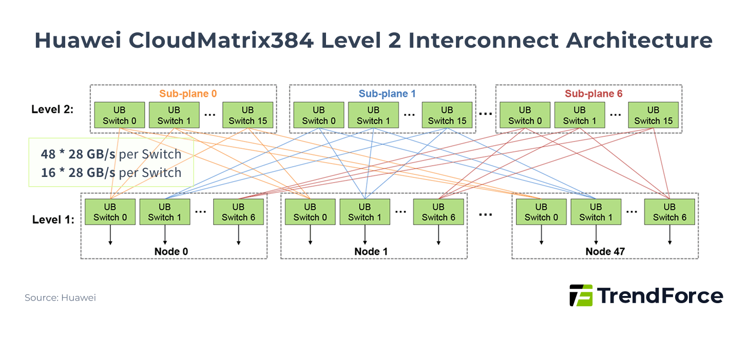
More strategically, Huawei plans to launch the Atlas 950 SuperPOD in 2026, which will adopt the next-generation UB 2.0 protocol and aims to provide massive interconnects for 8,192 NPUs. This number not only far exceeds current mainstream deployments, but also signals Huawei’s strong ambitions in the ultra-large-scale model training market.
At the same time, Huawei announced that UB 2.0 will be open to external partners, a move similar in spirit to NVIDIA’s NVLink Fusion strategy, aimed at standardizing its technology and expanding its ecosystem influence into other XPU markets.
China’s Open Standards Driving Scale-Up Market Development
In addition to Huawei’s move from a closed to an open strategy, China is actively developing several open standards to reduce reliance on a single supplier.
- ALS: Led by Alibaba and AMD, the alliance includes over ten members, such as Broadcom and Intel. Similar in concept to AMD’s UALink protocol, ALS aims to encourage diversified competition in the Scale-Up space through an open alliance model.
- ETH-X: Led by Tencent with more than thirty members, this standard focuses on improving Ethernet architectures and uses RoCE technology to boost bandwidth. Unlike ALS, ETH-X optimizes transmission encoding for greater efficiency. While this approach supports high bandwidth, it may also increase computational complexity and latency. In this sense, ETH-X is comparable to Broadcom’s SUE (Scale-Up Ethernet) protocol.
Table 4. NVLink vs. China’s Scale-Up Technologies
| Technology | NVLink 5.0 | UB 1.0 | ALS | ETH-X |
|---|---|---|---|---|
| Launch | 2024 | 2Q25 | 4Q24 | 4Q25 |
| Lead | NVIDIA | Huawei | Alibaba | Tencent |
| Topology | Clos | Clos | Clos | Clos |
| Bidirectional Bandwidth / Port | 800 Gbps | 800 Gbps | 800 Gbps (UALink) | 800 Gbps |
| Number of Nodes | 576 | 384 | 1,024 (UALink) | 64 |
| Latency | <1 μs | <2 μs | <1 μs | <1 μs |
| Ecosystem | Closed (before NVLink Fusion) | Closed (UB 2.0 moving to open) | Open | Open |
(Source: TrendForce)
Performance to Ecosystem: The Ultimate Battlefield of AI Chips
The battle over AI accelerators reveals a clear trend: pure hardware performance is no longer the sole deciding factor.
NVIDIA recently launched NVLink Fusion, enabling customers to integrate NVLink into their own ASICs. Meanwhile, Huawei announced that its UB 2.0 protocol will be opened to the public. These moves highlight a strategic shift: AI chip leaders are moving the battlefield from pure hardware performance to deeper ecosystem and software advantages.
NVIDIA knows that while its GPUs still dominate the high-end training market, maintaining its leadership requires locking customers further into its architecture through the unmatched CUDA ecosystem. This “strategic trade-off” sacrifices some hardware control in exchange for broader influence over software and toolchains.
At the same time, the ASIC camp, led by Broadcom, is promoting open standards to give CSPs alternatives beyond single-vendor solutions. Chinese giants such as Huawei and Alibaba are actively building independent domestic ecosystems, aiming to replicate NVIDIA’s success.
The future market leaders will be those offering the most complete and user-friendly hardware-software integration. In this battlefield, victory will no longer be defined by the performance of a single chip but by the breadth, depth, and stickiness of the ecosystem.
AI ASIC Market Outlook: Cloud Giants' Deployment and Competitive Edge
Cloud giants are accelerating the development of in-house AI ASICs, sparking a boom in market scale and projects. In 2026, next-generation ASICs are set to ramp up fully, marking a critical turning point for AI infrastructure. Get Trend Intelligence