[News] AI Interposers Grow Larger, Raising HBM4E Cooling Challenges: How Samsung, SK hynix Are Responding
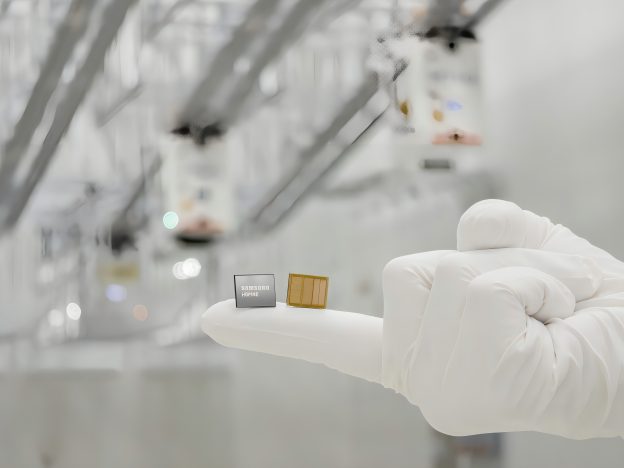
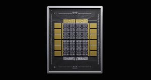
As AI packages expand to accommodate more compute and memory, managing heat is becoming increasingly important for next-generation HBM. According to Chosun Biz, the interposers connecting compute chips and HBM are expected to grow dramatically in size, while Samsung Electronics is preparing a range of technologies to address mounting thermal challenges in HBM4E, which it plans to begin mass-producing next year.
The scale of interposers is expected to increase significantly. The report notes that current AI interposers are already around 5.5 times the 858 mm² maximum area that an EUV lithography system can expose in a single shot. At the current pace, an official from the semiconductor equipment industry expects interposers carrying HBM to expand to nine times, 12 times, and eventually as much as 40 times that area.
The expansion reflects the limits of process scaling and the growing adoption of chiplet-based 2.5D packaging. As the report points out, a single chip manufactured using even the most advanced processes is increasingly unable to meet the massive computing requirements of AI workloads. Advanced AI systems are therefore combining multiple compute chiplets and HBM stacks on an interposer, allowing more compute and memory to be integrated into a single package.
Samsung Turns to HCB and HPB to Tackle HBM4E Heat
In response, Samsung is exploring several ways to improve heat dissipation, starting with lower-power designs. According to the report, key technologies under consideration include hybrid copper bonding (HCB) and heat path block (HPB).
HCB replaces the microscopic bumps between stacked DRAM dies with direct copper-to-copper connections. By reducing the gaps between layers, the technology can make the overall stack thinner while improving heat dissipation, the report notes. Samsung showcased HCB at NVIDIA’s GTC 2026 in March. HPB, meanwhile, offers an alternative way to reduce heat without requiring hybrid bonding.
Samsung is also taking a more targeted approach with HPB. At COMPUTEX 2026, the company identified the D2D PHY in HBM’s base die, which handles high-speed data transfers between HBM and the GPU, as a major source of heat. HPB creates a dedicated thermal path around this area to dissipate heat more efficiently and reduce thermal resistance. Samsung is currently validating the technology with HBM4E and plans to introduce it with HBM5.
SK hynix is pursuing a similar approach to localized HBM cooling. According to ETNews, its iHBM technology places highly thermally conductive but electrically insulating cooling material around the D2D PHY, where heat is concentrated, creating a dedicated path for heat dissipation. The company expects the design to reduce thermal resistance by around 30%.
Read more
- [News] Samsung Sees HBM Taking Nearly 30% of Industry DRAM Capacity in 2027, Up From 20% Currently
- [News] Samsung Reportedly Shifts Cheonan Capacity to HBM Packaging, Outsource Conventional Memory Modules
(Photo credit: Samsung)