[News] Intel Claims Industry’s Only High-Volume 300mm InP Silicon Photonics Capability as CPO Gains Momentum

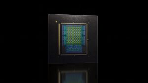
Intel is expanding its silicon photonics capabilities as demand for high-bandwidth optical interconnects grows across AI and high-performance computing (HPC). According to Wccftech, at the 2026 Open Compute Project (OCP) Global Summit, Intel claimed to be the only high-volume foundry capable of supplying 300mm indium phosphide (InP) silicon photonics at scale to the broader industry. The technology is intended to support next-generation near-package optics (NPO) and co-packaged optics (CPO) for AI and HPC applications.
As highlighted by ijiwei, conventional InP substrates are generally limited to 150mm (6-inch) wafers, with 3-inch and 4-inch formats still widely used, compared with the 300mm standard in silicon-based CMOS manufacturing. InP crystals are brittle, grow slowly, and present defect-control challenges, limiting laser chip output per wafer and slowing capacity expansion. To address these limitations, Intel integrates InP-based laser technology into its 300mm silicon photonics manufacturing platform, aiming to improve production efficiency and scalability.
NVIDIA, Broadcom, and TSMC Advance CPO Commercialization
Intel’s push comes as CPO commercialization begins to gain momentum. According to TrendForce, NVIDIA has begun shipping its Spectrum-X CPO switches to select partners, while Broadcom continues limited shipments of its 51.2 Tb/s Bailly CPO switches. Developed jointly with TSMC, NVIDIA’s Spectrum-X CPO switches use the foundry’s Compact Universal Photonic Engine (COUPE) technology.
Broadcom is also expanding its CPO portfolio. At OCP 2026, the company showcased its third-generation Tomahawk 6-Davisson CPO switch, offering 102.4 Tb/s of switching capacity and 200 Gbps per channel. TSMC, meanwhile, plans to begin production of its COUPE-on-substrate solution in 2026, targeting twice the power efficiency and a tenfold reduction in latency compared with board-level pluggable optics.
Chinese suppliers and cloud providers are also advancing NPO and CPO development. According to ijiwei, Zhongji Innolight has established a dedicated CPO production line and begun small-volume production of 800G CPO optical modules. Some customers have placed orders, with shipments potentially beginning in 2027 and broader adoption expected in 2028. Chinese cloud providers are also making progress. In September 2026, Huawei introduced its NPO-based Ascend 960 supernode for large-scale AI training and inference.
CPO Testing Emerges as a Key Mass Production Bottleneck
Despite progress toward commercialization, testing remains a key obstacle to CPO mass production. According to TrendForce, while optical alignment times have fallen to seconds or less, complete testing of a single photonic integrated circuit (PIC) can still take more than 100 seconds, shifting the bottleneck toward testing speed and cost. TrendForce expects 2027 to be a pivotal year for integrating CPO testing systems, with 2028 marking a critical period for assessing readiness for large-scale production.
Read more
- Integrated Optical-Electrical Testing Platforms Become Key to CPO Mass Production, Reshaping the Test Equipment Supply Chain, Says TrendForce
- [News] JEDEC Unveils First Industry-Wide Silicon Photonics Reliability Standard, Setting Rules Across Four Key Areas
(Photo credit: Intel)