[News] Samsung Reportedly Eyes Early 2027 for 3D Cube-H Advanced Packaging Development, Featuring Hybrid Bonding
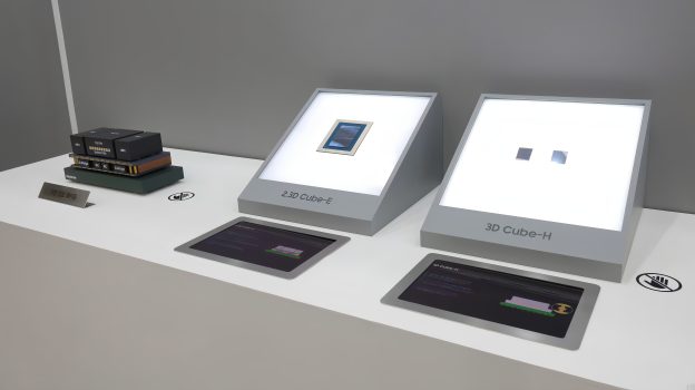
Samsung Electronics is accelerating its advanced packaging efforts as it looks to strengthen its position in AI chip manufacturing. According to ZDNet, citing industry sources, the company is aiming to complete development of its next-generation 3D Cube-H technology by early 2027. The technology uses hybrid bonding to enable vertical stacking of logic chips. Samsung plans to complete its first design kit in early 2027, followed by evaluations with potential customers.
The development could have broader implications for Samsung’s foundry business. As ZDNet notes, successful development of 3D Cube-H could strengthen the company’s competitiveness in next-generation AI semiconductors and lay the groundwork for securing manufacturing orders from major technology companies.
As the report explains, Samsung’s 3D Cube technology enables chips to be stacked vertically rather than arranged side by side, allowing greater transistor density within the same footprint. The company has already developed 3D Cube-T using thermocompression (TC) bonding and is now advancing 3D Cube-H, which adopts hybrid bonding to enable finer chip-to-chip connections.
Samsung has been developing 3D Cube-H with an interconnect pitch of approximately 6 micrometers (μm), significantly finer than the minimum pitch of around 25μm for existing TC bonding-based chips, ZDNet reports.
Unlike TC bonding, which joins chips through microscopic bumps using heat and pressure, hybrid bonding directly connects copper terminals between chips. The report notes that this approach enables denser interconnections, improving performance and energy efficiency while offering better thermal characteristics.
Samsung Advances AI Chip Stacking and Packaging R&D
3D Cube-H is expected to play a growing role in advanced AI chip packaging. According to ZDNet, potential applications include stacking high-performance logic chips such as GPUs, or integrating logic chips with memory devices such as HBM. However, hybrid bonding still faces technical challenges. According to ETNews, a Samsung packaging executive said at ISMP 2026 that controlling particle contamination and preventing void formation remain major hurdles in developing the technology.
Samsung is also expanding its advanced packaging research capabilities. According to Yonhap News, Chairman Jay Y. Lee visited the company’s Advanced Package Lab (APL) in Yokohama, Japan, on November 1 to review progress in packaging materials and process technologies. The facility, which officially opened in September, is part of a planned KRW 350 billion (US$262 million) investment over five years through 2028 to advance packaging R&D and strengthen collaboration with Japanese suppliers.
Read more
- [News] China’s NAURA Targets Hybrid Bonding With RMB 405M Deal as Domestic Equipment Push Accelerates
- [News] Samsung Reportedly Shifts Cheonan Capacity to HBM Packaging, Outsource Conventional Memory Modules
(Photo credit: Samsung)