[News] TSMC Plans Mini-Loop at Kaohsiung to Speed CoWoS Tool Validation; Reportedly Eyes AUO Site for CoPoS
As AI demand drives growth in advanced packaging, TSMC is strengthening equipment and materials validation across its supply chain. According to Commercial Times, construction of Kaohsiung’s Baipu Industrial Park began on September 21, with TSMC expected to anchor the cluster. The company plans to set up a modular “Mini-Loop” line to validate new equipment and process integration before the equipment is introduced into CoWoS (Chip-on-Wafer-on-Substrate) production, aiming to improve validation efficiency by 25% to 50%.
As the report highlights, the move could signal a more direct role for TSMC in coordinating its supply chain. TSMC Vice President of Advanced Packaging Technology and Service Jun He estimates that CoWoS capacity will grow at a compound annual rate of more than 80% through 2027, with growth continuing through 2029. Unlike major front-end equipment makers, many back-end equipment suppliers are smaller and have more limited R&D resources, making it increasingly difficult for them to conduct equipment and process validation independently as AI chips evolve rapidly.
Meanwhile, ASE reportedly plans to build two facilities at Baipu after breaking ground on a new Renwu facility in April. If the investment moves forward, it would bring TSMC’s equipment and materials validation platform closer to ASE’s packaging and testing capabilities, as the report points out.
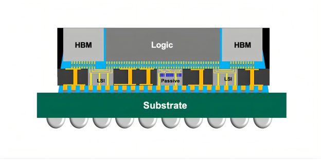
TrendForce notes that GPU suppliers and hyperscale CSPs are continuing to develop increasingly powerful and versatile AI chips, making larger package sizes a key development priority for 2.5D packaging. Although TSMC’s CoWoS-L faces competition from Intel’s EMIB-T, its advantages in technology maturity and yield are expected to keep it the mainstream packaging solution for AI chips through 2028.
TSMC Explores Glass Substrates as CoPoS Packaging Scales Up
TSMC is also reportedly exploring technologies for next-generation CoPoS as AI chips grow in size. According to another report from Commercial Times, the company is working to shift packaging substrates from round wafers to square panels while developing glass-core substrates. TSMC’s 3DIC R&D center in Japan is already developing glass-substrate technologies involving through-glass vias (TGVs), redistribution layers (RDLs), and GPU and HBM integration.
According to a July report from Economic Daily News, TSMC is currently building a CoPoS pilot line, with the technology and yields expected to take about another year to mature before production is introduced with customers.
Notably, TSMC has recently made multiple visits to AUO’s Central Taiwan Science Park facility, reportedly involving both a potential facility transaction and its CoPoS plans. The Commercial Times report notes that AUO’s experience in large-format panel processing, glass fabrication, and factory infrastructure overlaps with some of the capabilities required for panel-level packaging.
CoPoS Push Puts TGV and Inspection in Focus
For glass substrates, TGV formation is expected to become a key area of supply-chain competition. As Commercial Times highlights, the market currently favors ultrafast lasers combined with wet etching, using picosecond or femtosecond lasers to modify the glass before chemical etching forms the vias. Inspection is also expected to be a critical step in CoPoS mass production. The report notes that microcracks formed during laser drilling, copper plating, or thermal processing could spread to adjacent TGVs, affecting electrical performance and packaging yields.
Read more
- AI Chip Packaging Pushes Beyond Reticle Limits, with CoWoS-L Set to Remain the Mainstream Advanced Packaging Solution Through 2028, Says TrendForce
- [News] TSMC: SoIC, CoWoS to Drive 50× Compute by 2029; Silicon Photonics to Top 50% of Transceiver Market by 2027
(Photo credit: TSMC)