[Breaking] SMIC Eyes Backside Power for N7/N5 as AMEC ALD Tool Reportedly Clears Validation
As node scaling grows harder to sustain, foundries are turning to structural innovation to ease the resulting bottlenecks. This matters even more for Chinese chipmakers: without EUV access, they can’t rely on further shrinks to gain density or performance, making workarounds like backside power delivery (BSPD) increasingly critical. Against this backdrop, industry sources suggest leading domestic equipment makers are stepping up support for SMIC’s BSPD development for its N7/N5 processes.
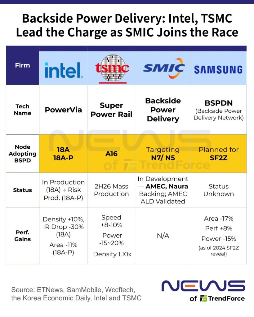
Notably, AMEC and Naura Technology are reportedly working with SMIC on BSPD for its N7/N5 nodes, with AMEC’s atomic layer deposition (ALD) equipment already clearing SMIC’s validation.
ETNews explains that in conventional chips, power and signal interconnects share the front side of the die. As nodes shrink, competition for routing space intensifies, worsening wiring congestion and resistance-induced voltage drops, the report notes, adding that backside power delivery can ease those constraints, but traditionally requires significant changes to transistor placement and standard-cell architectures.
Intel, TSMC Push Backside Power Into Leading-Edge Nodes
Foundry giants are already embracing backside power delivery for leading-edge chips, with Intel and TSMC at the forefront. Intel’s PowerVia, first deployed with 18A, shifts power routing to the backside of the wafer, freeing up the front for signal interconnects. Intel data cited by TechPowerUp shows the technology can boost density and cell utilization by up to 10% while cutting package-to-transistor IR drop by as much as 30%.
Intel is extending PowerVia to its 18A-P process, which is already in risk production, according to Wccftech. The upgraded node further capitalizes on backside power, delivering an 11% area reduction alongside shorter interconnects and fewer vias, the report adds.
TSMC is following a similar path with A16, pairing nanosheet transistors with its Super Power Rail backside power solution. Compared with N2P, TSMC says A16, expected to be production-ready in 2026, can deliver 8–10% higher speed at the same voltage, 15–20% lower power at the same speed, and up to 1.10X chip density—targeting HPC designs where complex signal routing and dense power networks make backside delivery increasingly valuable.
Citing industry source, ETNews reported in August that the foundry giant has successfully developed and validated A16, billed as the industry’s first angstrom-class CMOS platform featuring its Super Power Rail (SPR) backside power architecture.
As highlighted by ETNews, TSMC’s SPR stands out for its cleaner transition to backside power. It moves the power network entirely to the backside and feeds each transistor directly through dedicated vertical backside contacts (VBs), while requiring minimal changes to front-side structures and layouts.
Notably, earlier market chatters suggested that NVIDIA’s next-generation Feynman AI chips, expected to debut in 2028, are reportedly set to adopt TSMC’s latest A16 process.
On the other hand, ETNews reports that Samsung Electronics is also exploring backside power delivery for its SF2 process, potentially following an Intel-like approach. According to SamMobile, SF2Z, which features BSPDN technology, was unveiled back in 2024 but is absent from Samsung’s 2026 roadmap.
Read more
- [News] Huawei Reportedly Backs China’s DUV Drive, with 12 Systems Targeted by End-2026; SMIC Testing Underway
- [News] China’s Top Two Foundries Hit Capacity Crunch: What’s Next for SMIC and Hua Hong’s Expansion Plans?
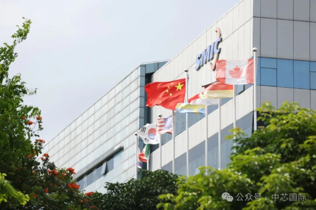
(Photo credit: SMIC)