[News] SK hynix Eyes EUV-Driven 6F² Scaling, Keeps 4F² and 3D DRAM in Play as Micron Holds Back
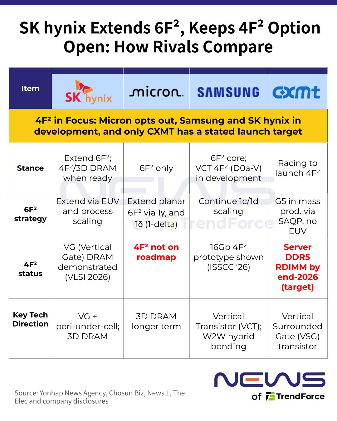
While Micron has ruled out adopting 4F² DRAM currently, saying the technology is “not on the roadmap right now,” SK hynix is keeping the door open. During its 3Q26 earnings call, the Korean memory giant said it plans to maximize the potential of its existing 6F² architecture through process improvements and stable platform operations, while continuing to develop 4F² and 3D DRAM as potential next-generation options, according to Yonhap News Agency.
As Chosun Biz explains, 4F² reduces the DRAM cell footprint from 3F × 2F in the conventional 6F² architecture to 2F × 2F, cutting cell area by 33%. Here, F denotes the minimum feature size of a semiconductor circuit.
But that density gain comes with trade-offs. Smaller cells do not necessarily improve manufacturing efficiency, as greater process complexity can drive up costs and hurt yields. This underpins Micron’s skepticism over 4F², Chosun Biz notes.
According to the report, Micron President and Chief Technology and Product Officer Scott DeBoer said more than 20 years of research had failed to identify a sustainable scaling path. While technically feasible, the 4F² structure’s process complexity and higher manufacturing costs limit its practical benefits, DeBoer noted.
SK hynix Leverages EUV to Extend 6F² DRAM’s Lifespan
According to News 1, SK hynix DRAM marketing head Park Joon-deok said advances in EUV lithography and process scaling offer further room to extend the 6F² platform. For now, the company sees maximizing the potential of its proven architecture—with established production stability and cost competitiveness—as the most efficient strategy.
Park stressed that commercializing new cell architectures requires more than performance gains, citing yields, reliability, costs, product design and customer validation as key hurdles. As Yonhap News Agency notes, SK hynix is pursuing a phased roadmap for 4F² and 3D DRAM, with adoption tied to each technology’s maturity and economic viability.
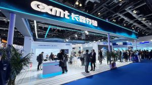
While SK hynix prioritizes extending its proven 6F² platform, China’s CXMT is pushing ahead with 4F² commercialization plans, aiming to launch its first 4F²-based server DDR5 RDIMM module by the end of 2026. If successful, the Chinese memory maker could gain an early foothold in a technology yet to be commercialized globally.
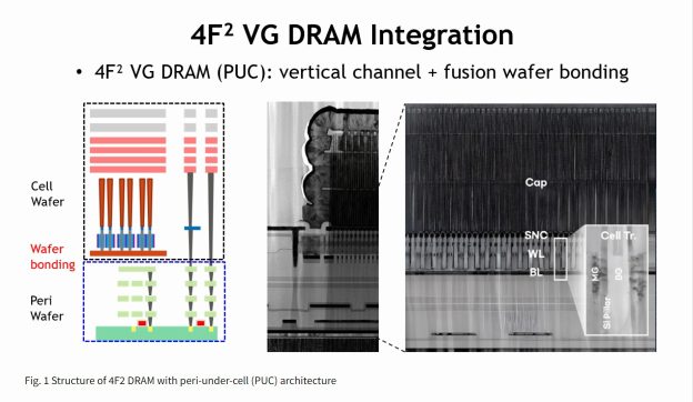
Indeed, SK hynix is also pursuing 4F² DRAM research. In a July research blog post tied to VLSI 2026, the company said conventional buried-gate cell transistors face scaling limits at sub-10nm nodes, and positioned 4F² vertical-gate (VG) DRAM as a way to extend scaling.
The work used a peri-under-cell (PUC) architecture, with the cell array and peripheral circuits joined through wafer bonding, and focused on two features. A shared back gate (BG) between adjacent word lines allows threshold-voltage tuning and curbs interference from neighboring word lines without enlarging the cell. Bit-line shielding (BLS), meanwhile, could cut bit-line coupling noise and sensing failures.
Similar to SK hynix’s approach, Samsung Electronics is developing a 4F² architecture based on vertical channel transistors (VCT), which reduce cell area by arranging transistors vertically rather than horizontally, Chosun Biz reports. Song Jae-hyuk, President and CTO of Samsung’s Device Solutions (DS) division, confirmed the company’s 4F² development efforts at SEDEX 2026 in Seoul on October 14, the report adds.
Read more
- [News] Micron Reportedly Rules Out 4F² DRAM Scaling, Backs 6F² and 3D DRAM in Next-Gen Memory Roadmap
- [News] CXMT Accelerates 4F² DRAM Push, Eyes Year-End Server DDR5 RDIMM Launch
(Photo credit: SK hynix)