[News] TSMC Pushes Back on 3D DRAM Rumors: Three Memory Plays Where It Still Has a Say

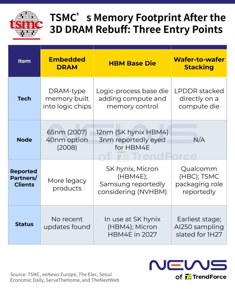
While TSMC has pushed back against 3D DRAM manufacturing rumors, reaffirming its commitment to its core foundry business, the chip giant is no stranger to memory-related technologies. Industry sources indicate that TSMC is involved in embedded DRAM, HBM base dies and wafer-to-wafer stacking for Qualcomm, despite having no concrete plans to manufacture DRAM itself. Here’s a closer look at these technologies and TSMC’s role in each.
Embedded DRAM: 65nm and 40nm
While advanced-node development has taken center stage in TSMC’s AI-driven strategy, the foundry has a long history with embedded DRAM (eDRAM), which places DRAM-type memory directly inside logic chips. In 2007, TSMC said it had produced its first 65nm eDRAM customer products. In March 2008, it said its new 40nm 40G and 40LP processes could be paired with embedded DRAM, alongside mixed-signal and RF options, according to TSMC.
More recently, TSMC’s disclosed embedded-memory work has centered on non-volatile technologies. Its website lists Flash, Spin-transfer torque magnetic random access memory (STT-MRAM), and resistive random access memory (RRAM) among its non-volatile memory solutions. eeNews Europe reported back in 2025 that its 22nm MRAM is in production, with 16nm ready for customers and 12nm in development.
HBM Base Dies Open New Opportunities for TSMC’s Advanced Nodes
As cloud service providers (CSPs) accelerate in-house AI chip development, growing interest in custom HBM is creating fresh opportunities for TSMC’s advanced logic processes. According to TrendForce, HBM base dies are expected to increasingly adopt the foundry giant’s advanced nodes starting with HBM4E. While some suppliers may turn to TSMC’s 12nm process for standard HBM products, customized designs could push further into 3nm territory, TrendForce observes.
SK hynix and Micron are reportedly poised to tap TSMC for custom HBM4E base die production. According to The Elec, Scott J. DeBoer, Micron’s president and chief technology and products officer (CTPO), revealed at the company’s September 30 earnings event that both its NVIDIA co-designed NVHBM and JEDEC-standard HBM4E are being developed using foundry-manufactured base dies. The move marks a departure from Micron’s HBM4 approach, which relied on an internally developed base die.
More strikingly, the trend could bring even Samsung, a direct foundry rival, into TSMC’s orbit. According to Seoul Economic Daily, NVIDIA has asked Samsung, SK hynix and Micron to use TSMC’s 3nm process for the base dies of its NVHBM, unveiled in August. The move reportedly aims to standardize manufacturing across suppliers, ensuring consistent performance and streamlining product validation.
Wafer-to-Wafer Bonding for Qualcomm’s HBC May Create an Opening for TSMC
On the other hand, Qualcomm is advancing a different approach to memory integration, having validated its first chips featuring High Bandwidth Compute (HBC) technology in early November. First unveiled earlier this year, HBC is expected to debut in Qualcomm’s Dragonfly AI250 accelerator, with sampling slated for 1H27, according to ServeTheHome.
Unlike conventional HBM, which connects memory stacks to a separate processor, HBC places LPDDR memory directly atop the compute die, bringing data closer to processing units, ServeTheHome notes, adding that the architecture aims to curb data movement and power consumption while potentially reducing manufacturing costs. Notably, according to TheNextWeb, the development involved collaboration with foundry and assembly partners on wafer-to-wafer bonding, enabling memory to be stacked directly onto logic chips.
Against this backdrop, TSMC could also have a role in bringing HBC to market. According to an August report by The Elec, Samsung and SK hynix are working with Qualcomm on the technology’s commercialization, with both memory giants expected to handle DRAM stacking. TSMC, meanwhile, is reportedly poised to contribute its expertise in technology integration and advanced packaging.
Taken together, these developments suggest that TSMC may not need to manufacture DRAM to capitalize on the memory boom. From HBM base dies to wafer-to-wafer bonding, its advanced logic and packaging capabilities could give the foundry giant an increasingly important role in next-generation memory integration—even as it stays firmly out of conventional DRAM production.
Read more
(Photo credit: CXMT)