[News] Samsung Reportedly Plans KRW 46T Onyang HBM Hub with Five Lines, Moves Up Operations by One Year to 2028
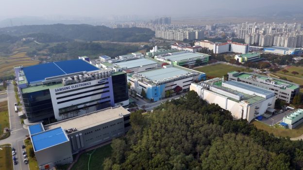
Samsung Electronics is accelerating its investment in high-bandwidth memory (HBM) amid surging demand for AI chips. According to Chosun Biz, Chairman Lee Jae-yong outlined plans to transform the company’s Onyang Campus in Asan, South Chungcheong Province, into a major HBM production hub, with operations at its new facility moved up by about a year to June 2028. Meanwhile, Asia Business Daily reports that HBM mass production is expected to begin in May 2029.
As Yonhap News notes, Samsung plans to invest KRW 46 trillion to establish five HBM production lines at Onyang, including KRW 6 trillion for factory construction and KRW 40 trillion for advanced equipment, with spending to be carried out in phases. Upon completion, the Onyang Campus’s total floor area will increase from 270,000 to 420,000 square meters, or roughly 1.6 times its current size.
The new Line 5 facility will feature three floors of cleanroom space totaling approximately 31,000 square meters. According to Chosun Biz, the facility is expected to produce next-generation HBM products, including seventh-generation HBM4E, as Samsung seeks to secure advanced packaging capacity amid rising demand for AI server memory.
Separately, Seoul Economic Daily reports that Samsung has raised its broader investment plan for Onyang and Cheonan from KRW 56 trillion to KRW 60 trillion, aiming to strengthen HBM production and advanced packaging capabilities across both sites.
Samsung Prioritizes HBM Packaging in Broader Expansion Push
Samsung is also prioritizing HBM packaging capacity at its existing facilities. According to an earlier report by The Elec, the company is reportedly reallocating space and equipment at its Cheonan and Onyang sites toward advanced packaging, including HBM, while outsourcing more conventional memory module production.
The Onyang expansion also forms part of broader investment plans announced by Samsung affiliates in July, Reuters reports. The project supports South Korea’s wider industrial development initiative in the Chungcheong region, where the government is working with Samsung, SK hynix, and other companies on major projects spanning semiconductors, physical AI, and AI data centers.
Read more
- [News] Samsung Reportedly Eyes Early 2027 for 3D Cube-H Advanced Packaging Development, Featuring Hybrid Bonding
- [News] Samsung, SK hynix Reportedly Race for ASML EUV Amid 2027–2028 Shortages; Orders Worth Up to KRW 20T Each
(Photo credit: Samsung)