[News] NVIDIA Reportedly Pushes TSMC 3nm NVHBM Base Dies for Samsung, SK hynix, Micron, Uniting Foundry Rivals
As previously reported by ZDNet in September, Samsung is pursuing a dual-track strategy for custom HBM, tapping both its own foundry and rival TSMC for base die production. A new report from Seoul Economic Daily lends further weight to this strategy, revealing that NVIDIA has asked Samsung, SK hynix and Micron to adopt TSMC’s 3nm process for the base dies of its NVHBM, unveiled in August.
The move brings two fierce foundry rivals, Samsung and TSMC, into closer cooperation despite their competition for major customers such as Qualcomm and Tesla. According to Seoul Economic Daily, NVIDIA’s push to standardize production across suppliers is aimed at ensuring consistent HBM performance while simplifying product validation. Samsung’s Device Solutions (DS) division, which oversees its foundry business, reportedly agreed to the requirements following an internal review.
Beyond manufacturing consistency, TSMC’s yield advantage appears to be another key factor. A separate Seoul Economic Daily report notes that NVHBM’s complex base die design requires advanced logic technology, with industry estimates placing TSMC’s 3nm yields above 90%, versus around 60% for Samsung Foundry’s 2nm (SF2) process.
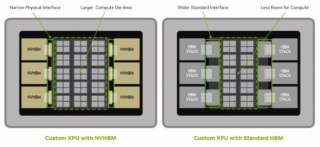
NVHBM’s custom base die integrates the memory controller traditionally housed in the GPU, underscoring the need for advanced logic processes. According to NVIDIA, the technology offers up to 30% more memory bandwidth, 15% lower HBM power consumption and 25% more XPU compute die area than standard HBM4E.
The partnership is not entirely new, however. According to Seoul Economic Daily, Samsung and TSMC first collaborated four years ago to ensure HBM compatibility with TSMC’s GPU packaging process. Their latest tie-up, however, takes the relationship a step further, extending it into HBM manufacturing for the first time.
Samsung Keeps Its Own Foundry in Play for NVHBM Base Dies
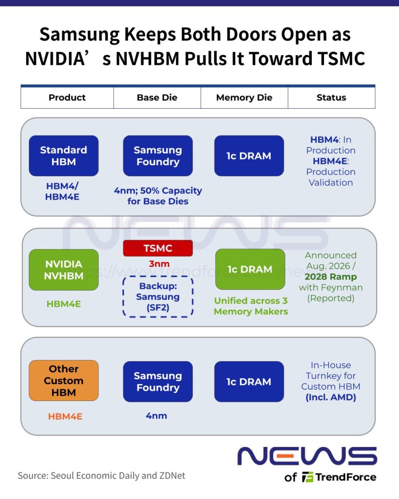
Still, Samsung is keeping its own foundry in the picture. According to Seoul Economic Daily, with TSMC’s 3nm capacity facing competing demand from AI accelerators and smartphone chips, Samsung is validating NVHBM base die production on its 2nm process as a potential alternative should TSMC face capacity constraints.
Indeed, TSMC flagged tight 3nm capacity at its October 15 earnings call, with the node accounting for 33% of third-quarter wafer sales, its largest share among all process nodes. According to Economic Daily News, Chairman and CEO C.C. Wei announced plans for another 3nm fab in Tainan, on top of existing expansion projects in Arizona, Japan’s Kumamoto and Taiwan’s Southern Taiwan Science Park. The additional fab is slated to begin mass production in the first half of 2028.
Beyond NVHBM, Samsung remains committed to producing base dies in-house for its standard HBM lineup. According to Seoul Economic Daily, both its HBM4, which entered mass production earlier this year, and HBM4E, now undergoing production validation, use Samsung Foundry’s 4nm process for base dies, while their core dies are manufactured on 1c DRAM lines at its Hwaseong and Pyeongtaek campuses.
Samsung also plans to maintain its turnkey approach to base die production for custom HBM supplied to other customers, including AMD, while exploring its own 2nm process as an alternative for NVHBM, the report adds.
Read more
- [News] NVIDIA’s NVHBM Reshapes Base Die Strategies: How Micron, Samsung Are Bringing TSMC Into the Fold
- [News] NVIDIA’s Supply Commitments Soar to $279B as Memory Costs Surge; New NVHBM Boosts Bandwidth 30%
(Photo credit: NVIDIA)