[News] Intel Reportedly Touts 90%+ Wafer Utilization with Interposer-Free EMIB, Eyes 70+ Bridges per Future AI Chip
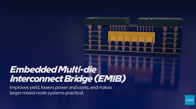
With TSMC’s CoWoS capacity running tight, Intel is spotlighting its advanced packaging technologies, Embedded Multi-die Interconnect Bridge (EMIB) and EMIB-T, as an alternative. According to ZDNet Korea, Kyu-oh Lee, Intel’s Director of Foundry Packaging, said EMIB uses small, localized silicon bridges instead of a full-size interposer, achieving silicon wafer utilization of over 90%, versus roughly 60% for interposer-based designs.
As explained by the report, unlike conventional silicon interposers, EMIB uses small silicon bridges to connect chips, placing them only where needed for greater cost efficiency. In particular, EMIB-T, which integrates through-silicon vias (TSVs) into the bridges to enable power delivery, has drawn positive industry attention, the report notes.
The technology is, therefore, reportedly gaining traction among major U.S. tech firms. Industry sources suggest Google’s TPU v9 lineup could adopt Intel’s EMIB-T for both HumuFish and TriggerFish, while WhaleFish is expected to use TSMC’s CoWoS-L. On the other hand, Amazon is also reportedly planning to incorporate EMIB-T into its custom AI chips, according to ZDNet.
Larger AI Chip Packages Could Drive EMIB Bridge Count Beyond 70
Beyond potential customer adoption, the shift toward larger AI chip packages could provide another growth opportunity for Intel’s EMIB technology. According to Lee, cited by ZDNet Korea, AI chips commercialized in 2026 feature packages measuring up to 120 × 120 mm, integrating 12 HBM stacks and more than 20 EMIB bridges.
And the numbers are set to climb. AI chips currently under development are targeting packages of at least 120 × 180 mm, with 16 or more HBM stacks and at least 38 bridges. Looking further ahead, Intel envisions 240 × 240 mm packages integrating over 32 HBM stacks and more than 70 EMIB bridges, Lee noted.
The rising bridge count could also create opportunities further down Intel’s supply chain. As previously reported by the Economic Daily News, Taiwanese foundry UMC manufactures EMIB silicon bridges using mature 12-inch wafer processes at its fabs in Taiwan and Singapore.
TSMC, meanwhile, is pursuing a similar push toward larger AI chip packages through its CoWoS technology. According to TrendForce, the foundry giant’s CoWoS-L is expected to support a 5.5X reticle-size package integrating four chiplets and 12 HBM stacks in 2026. By 2028, the technology is projected to scale to 14X, accommodating 20 chiplets and 20 HBM stacks.
Read more
- [Breaking] Google Reportedly Sticks With Intel EMIB-T Despite 35% Substrate Yields as HumuFish Schedule Tightens
- [Breaking] Intel EMIB Substrate Yields Reportedly Hit 45%, Suppliers Eye 60% by 1Q27
(Photo credit: Intel)