[News] Qualcomm Completes HBC Validation, Claims 5×+ HBM4 Bandwidth Efficiency; AI250 Sampling in 1H27
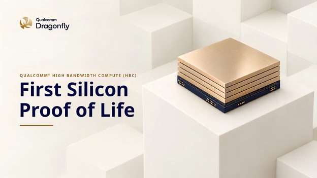
Qualcomm has completed initial hardware validation of its first-generation High Bandwidth Compute (HBC) technology, marking a key step toward commercialization. According to ServeTheHome, the company has successfully tested HBC’s memory read-write and near-memory computing capabilities. The technology, first unveiled earlier this year, is set to debut in Qualcomm’s Dragonfly AI250 accelerator, scheduled to begin sampling in the first half of 2027.
HBC stacks LPDDR memory directly on a compute die, allowing data to be processed closer to where it is stored. Unlike conventional HBM, which connects memory stacks to a separate processor, the design aims to reduce data movement and power consumption while potentially lowering manufacturing costs, the report explains.
The latest validation provides early evidence of HBC’s performance potential. According to ServeTheHome, Qualcomm measured bandwidth-per-watt efficiency at more than five times that of HBM4, based on a comparison with HBM4 specifications. The company also reported 18 times the bandwidth of external LPDDR5X, although it has not disclosed specific bandwidth figures.
HBC Targets Lower Packaging Costs and Higher Memory Capacity
HBC also aims to reduce packaging costs and complexity. As ServeTheHome explains, conventional HBM requires advanced packaging technologies such as CoWoS or EMIB to connect memory stacks with compute dies and controllers through an ultra-wide interface. By moving much of the computation to the die beneath the memory stack, HBC reduces the bandwidth needed to communicate with the main processor, potentially enabling less expensive packaging solutions such as conventional 2D organic substrates.
HBC also uses LPDDR5X DRAM dies instead of the specialized DRAM dies used in HBM, potentially reducing costs. While Qualcomm has yet to disclose final performance specifications, HBC stacks are expected to offer greater memory capacity than current HBM4 implementations, according to ServeTheHome.
Qualcomm’s HBC development could also involve major semiconductor suppliers. As previously noted by The Elec, Samsung Electronics and SK hynix have reportedly been working with Qualcomm on HBC commercialization, while TSMC is expected to support technology integration and advanced packaging. However, the companies have yet to publicly confirm specific production arrangements.
Looking ahead, Qualcomm plans to extend HBC to its next-generation Dragonfly AI300 accelerator. According to the company‘s June announcement, AI300 will feature second-generation HBC technology, targeting 54 times the effective memory bandwidth of the LPDDR5X-based AI200, with sampling expected in 2028.
Read more
- [News] Qualcomm Reportedly Enlists Samsung, SK hynix as HBC Memory Partners; TSMC Eyes Packaging Role
- [News] SK hynix Eyes EUV-Driven 6F² Scaling, Keeps 4F² and 3D DRAM in Play as Micron Holds Back
(Photo credit: Qualcomm)