[News] Former Intel CEO Pat Gelsinger Backs Memory Startup Eyeing EUV-Free Z2RAM, Targets Samples Within 4 Years
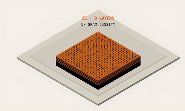
Former Intel CEO Pat Gelsinger is backing a memory startup developing Z2RAM, a technology targeting SRAM-like speed and DRAM-like density to address AI computing’s memory bottleneck. According to The Register, Nagare Labs recently secured US$5 million in seed funding led by Playground Global, where Gelsinger became a partner last year. Founded by Georgia Institute of Technology researchers Suman Datta and Shimeng Yu, Nagare Labs builds on years of research into next-generation memory technologies, including ferroelectric and resistive RAM.
Z2RAM uses oxide semiconductors and is designed for direct integration on top of logic chips through 3D hybrid bonding, according to Nagare Labs. Semicon Leaders Asia adds that the technology is designed to use standard back-end-of-line (BEOL) processes, allowing multiple memory layers to be formed through a single lithography exposure without requiring EUV. This approach could increase memory density while reducing manufacturing complexity and costs.
The technology remains at the laboratory prototype stage. As noted by The Register, Nagare Labs is seeking an R&D fabrication partner to scale production beyond university cleanroom facilities. The startup plans to sample working Z2RAM memory tiles within four years, with commercial shipments targeted within the next decade.
Z2RAM Targets Higher Density Through Transistor-Based Memory
As noted by The Register, Z2RAM targets more than five times the bit density of SRAM in its initial implementation. While its capacity would remain far below that of HBM-equipped accelerators such as NVIDIA’s Rubin, with 288GB of memory, and AMD’s MI455X, with 432GB, the technology could offer a significant density improvement over SRAM-based accelerators such as NVIDIA’s Groq LPUs.
Unlike conventional DRAM, which relies on capacitors to store charge, Z2RAM uses transistor-based memory cells that enable non-destructive reads, potentially reducing memory access latency, the report explains. Nagare Labs is also developing a process to stack these cells vertically, similar to the layered structure of NAND flash.
Integration Standards and Reliability Remain Key Challenges
Nagare Labs is open to working directly with chipmakers to integrate Z2RAM into their designs, but technical hurdles remain. As The Register points out, there is currently no established industry standard for connecting this type of memory to AI accelerators through 3D hybrid bonding. Without such a standard, Nagare Labs may need to develop its own interface to realize Z2RAM’s potential capacity and speed advantages, adding complexity to commercialization.
Reliability also requires further validation. While oxide semiconductors offer advantages in thermal and radiation performance, they are susceptible to atomic vacancies, posing another challenge as the technology moves toward production, The Register notes.
Read more
- [News] Micron Reportedly Rules Out 4F² DRAM Scaling, Backs 6F² and 3D DRAM in Next-Gen Memory Roadmap
- [News] Intel and Memory: A History of Exits, and a New Bid to Return
(Photo credit: Nagare Labs)