[News] Samsung 2nm Taylor Fab 2 Reportedly Fully Booked Before 2030 Output, Led by AMD HBM Base Die Orders
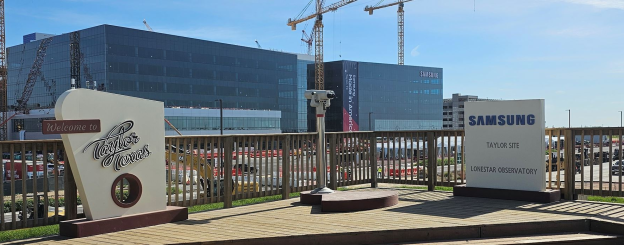
Samsung Electronics is reportedly gaining momentum in its U.S. foundry expansion, with its second plant in Taylor, Texas, reportedly set to produce HBM base dies for AMD and NVIDIA. According to Maeil Business Newspaper, citing industry sources, Samsung has secured orders covering the entire planned production capacity of Taylor Fab 2, with AMD accounting for the majority. Sources indicate that the facility’s capacity could be stretched even by AMD’s orders alone. Samsung plans to adopt a 2nm process at Taylor Fab 2, which will span 2.7 million square feet (approximately 250,000 square meters), about 1.5 times the size of Taylor Fab 1, the report adds.
Preparatory work, including site preparation and ground leveling, is already underway, with full-scale construction scheduled to begin in early November 2026. Equipment installation is expected to start in February 2029, followed by mass production in 2030, according to the report.
Once production begins, Samsung plans to combine base dies manufactured at Taylor Fab 2 with DRAM produced in South Korea to supply completed HBM products, the report notes. While its mass-produced HBM4 and sampled HBM4E use 4nm base dies, the new facility could manufacture base dies using 2nm or more advanced processes to meet next-generation HBM demand.
Samsung could also expand its customer base. In a separate report, Maeil Business Newspaper notes that industry observers see Broadcom as another potential customer for HBM base dies from Taylor Fab 2. Beyond HBM base dies, Samsung is pursuing broader AI chip manufacturing opportunities. According to ChosunBiz, Samsung could manufacture 2nm AI chips for a U.S. cloud customer through Taiwan-based ASIC design firm Faraday. The potential project could help Samsung attract customers seeking alternatives to TSMC, although manufacturing orders remain unconfirmed.
The reported orders come as Samsung’s foundry business shows signs of improvement. According to Reuters, Samsung said its third-quarter foundry revenue benefited from HBM logic die sales and advanced 2nm orders from hyperscalers and other AI customers, although the business remains loss-making.
NVIDIA’s NVHBM Strategy Could Pose Challenges for Samsung Foundry
Despite the reported orders, Samsung faces uncertainty over its role in NVIDIA’s next-generation customized HBM supply chain. Maeil Business Newspaper reports that Samsung is evaluating whether its own foundry processes could produce base dies for NVIDIA’s NVHBM, potentially providing an alternative if TSMC’s capacity falls short of demand. However, NVIDIA has reportedly asked all three major memory manufacturers, including Samsung, to outsource NVHBM base die production to TSMC.
As NVIDIA supplies multiple generations of graphics processing units (GPUs) simultaneously, conventional HBM and NVHBM could coexist during the transition. Nevertheless, wider NVHBM adoption could limit Samsung Foundry’s opportunities to secure additional base die orders if NVIDIA continues to favor TSMC as its manufacturing partner, as noted by Maeil Business Newspaper.
Read more
- [News] Samsung Reportedly to Exit 8-Inch Foundry by 2030 as TSMC Also Cuts Capacity
- [News] Samsung Sees 8nm-and-Below Utilization Topping 100% in 2027; 2nm Projects to More Than Double
(Photo credit: Samsung)