[News] Samsung Reportedly Expands zNAND Lineup With zNAND-T and zNAND-I for AI Data Centers and Inference
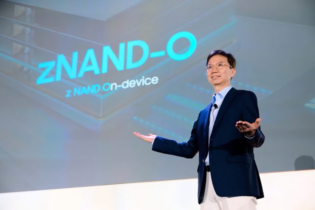
As AI workloads drive demand for more specialized memory solutions, Samsung Electronics is reportedly expanding its next-generation NAND flash portfolio to meet different performance requirements. According to ZDNet, citing industry sources, the company is in the early stages of developing three zNAND products: zNAND-O, zNAND-T, and zNAND-I, each targeting different AI applications.
While Samsung has yet to officially announce zNAND-T and zNAND-I, both are reportedly under development. zNAND-T focuses on maximizing throughput and bandwidth for high-capacity, high-performance AI data centers. Similar to zNAND-O, it uses vertically stacked NAND dies connected through-silicon vias (TSVs), an architecture commonly associated with high-bandwidth flash (HBF), the report notes.
Meanwhile, zNAND-I is designed to maximize input/output operations per second (IOPS), a measure of how many read and write operations a storage device can complete each second. Unlike bandwidth, which measures how much data can be transferred over a given period, IOPS reflects how frequently individual operations can be performed. According to the report, this makes high-IOPS NAND particularly suitable for AI inference workloads that require frequent access to small amounts of temporary data, such as key-value (KV) caches.
Samsung Targets 2028 zNAND-O Samples With TSV-Based Design
Samsung previously unveiled a mockup of zNAND-O at a memory industry event in the U.S. in August. Designed for on-device AI, zNAND-O uses TSVs to vertically stack four or eight NAND dies, shortening data transmission paths to improve speed and power efficiency, the report notes.
Building on this design, Samsung aims to achieve 10 times the bit density of DRAM and seven times the read bandwidth and power efficiency of conventional NAND with zNAND-O, according to NewsPim. The product is designed to combine DRAM-like speed with NAND’s high storage capacity, addressing growing data-processing demands from generative AI and large language models (LLMs). Samsung plans to begin supplying zNAND-O samples in 2028, the NewsPim report adds.
SK hynix Develops Three AI-NAND Products Targeting Performance, Density, and Bandwidth
Samsung is not alone in developing NAND products tailored to different AI workloads. According to ZDNet, SK hynix established its AI-NAND (AIN) family in the second half of 2025, comprising three categories: AIN P (Performance), AIN D (Density), and AIN B (Bandwidth). AIN P focuses on performance, with SK hynix developing products targeting up to 100 million IOPS. AIN D prioritizes SSD storage density, aiming for capacities of up to the petabyte (PB) level. AIN B, meanwhile, focuses on improving bandwidth, much like HBF.
Read more
- [News] Samsung 3Q Preliminary Results Preview: Market Sees Historic KRW 100T Profit, Memory Margin Could Top 80
- [News] Sandisk Reportedly Tapes Out First HBF Product, Targets 2027 Samples and 2028 Production
(Photo credit: Samsung)