[News] TSMC’s $2B Silicon Interposer Deal with GF Could Fast-Track U.S. Packaging to 1H28, Free Up Fab Capacity

Ahead of TSMC’s earnings call this Thursday, its $2 billion silicon interposer manufacturing deal with U.S. foundry GlobalFoundries is drawing attention. As Commercial Times notes, silicon interposers do not require leading-edge nodes such as 2nm or 3nm. With its existing 65nm interposer platform, GlobalFoundries could carve out a role in the AI chip supply chain despite exiting the sub-7nm logic race, the report suggests.
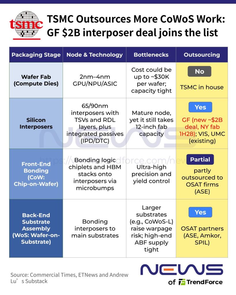
More notably, the deal could pave the way for TSMC to accelerate its U.S. advanced packaging ramp. According to Commercial Times, TSMC originally targeted 2029 for establishing CoWoS and 3D IC packaging capabilities in Arizona. With GlobalFoundries set to ramp silicon interposer production in 1H28 and Amkor’s Arizona facility slated to open in early 2028, industry observers cited by the report suggest TSMC’s first U.S. advanced packaging plant could begin operations as early as 1H28, ahead of schedule.
Beyond the timeline, the deal could also carry strategic and geopolitical implications. As semiconductor analyst Andrew Lu suggests, the partnership could ease U.S. pressure on TSMC over chips manufactured domestically but packaged in Taiwan. By bringing together TSMC’s Arizona-made 4nm and 3nm chips, with 2nm to follow, GlobalFoundries’ silicon interposers and Amkor’s packaging capabilities, the partnership could pave the way for a more localized U.S. CoWoS supply chain, Lu says.
The arrangement could also sharpen TSMC’s capital efficiency. As Lu argues, silicon interposers, typically made on mature 65nm or 90nm processes, contain few active transistors but still consume valuable 12-inch fab capacity.
By outsourcing this lower-margin work to GlobalFoundries, TSMC could focus on higher-value operations, from 3nm and 2nm compute dies reportedly priced at up to $30,000 per wafer to advanced chip-on-wafer (CoW) bonding.
Tom’s Hardware further explains that interposer fabrication is just one step in the CoWoS-S process. The technology also involves precision bonding of logic chiplets and HBM stacks, assembly onto organic substrates, and electrical testing—all requiring dedicated capacity not covered by the TSMC–GlobalFoundries deal.
AI Interposer Boom Fuels Taiwan Foundries’ Expansion
Meanwhile, the AI packaging boom is creating fresh opportunities for Taiwan’s mature-node foundries, with UMC and PSMC expanding beyond traditional chipmaking into silicon interposers and other advanced packaging components.
According to Economic Daily News, UMC plans to double its monthly silicon interposer capacity from 3,000 to 6,000 wafers to meet rising demand. Its 2.5D packaging solution featuring deep trench capacitors (DTC) is reportedly shipping to a major customer, while active interposers are undergoing validation with multiple clients.
UMC is also gaining traction in Intel’s advanced packaging supply chain. A separate Economic Daily News report highlights strong orders for its silicon bridges, which are embedded in substrates for Intel’s packaging technology.
On the other hand, the report notes that as Intel accelerates development of its 18A and 14A process nodes while expanding advanced packaging capacity, PSMC has secured a foothold in its EMIB supply chain through its long-established 12-inch integrated passive device (IPD) platform, serving as the exclusive supplier of silicon capacitors.
Read more
- [News] ASE’s SPIL Reportedly Nears Arizona Expansion as TSMC, Amkor Step Up U.S. Advanced Packaging Push
- [News] TSMC Reportedly Expands Outsourcing of Key CoWoS Front-End Step to OSATs Amid Rising NVIDIA, ASIC Demand
(Photo credit: TSMC)