[News] NVIDIA Reportedly Explores Glass Substrates, 2028 Adoption Possible as Taiwan Suppliers Step Up
As AI chips grow larger and more complex, glass substrates are emerging as a potential next step in advanced packaging. According to Commercial Times, NVIDIA is reportedly evaluating the technology for next-generation AI chip packaging, drawing growing attention to Taiwan’s display panel and glass processing supply chain. Still, industry sources note that process yields and customer qualification remain key hurdles to large-scale commercialization.
NVIDIA is reportedly engaging with the broader supply chain for potential adoption. Commercial Times, citing Seoul Economic Daily, notes that the company is exploring glass substrates with several partners, including German equipment maker SCHMID, as it seeks to further improve AI semiconductor performance. KIPOST adds that NVIDIA has asked substrate makers in South Korea, Japan, and Taiwan to complete development within two years, potentially paving the way for adoption before 2028.
NVIDIA is also reportedly pushing for broader industry development of the technology. Seoul Economic Daily notes that CEO Jensen Huang met with SK Group Chairman Chey Tae-won to discuss cooperation in next-generation semiconductor technologies, including glass substrates.
Taiwan Suppliers Step Up Glass Substrate Development
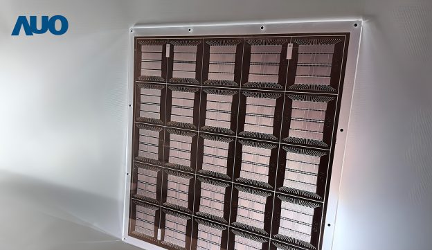
Taiwanese suppliers are also stepping up development efforts. As noted by Commercial Times, AUO is expanding into advanced semiconductor packaging by leveraging its large-format glass processing, precision metallization, and redistribution layer (RDL) capabilities. According to Liberty Times, AUO is planning pilot lines for TGV, RDL, and glass core technologies. Chairman Paul Peng said in July that the projects are included in the company’s NT$8.6 billion capital expenditure plan, while glass core technology could take another two to three years to reach a more mature stage.
At SEMICON Taiwan 2026, AUO and Corning also showcased a 510 × 515 mm glass core substrate combining Corning’s semiconductor-grade glass with AUO’s RDL processes to address high-density interconnect and low-loss transmission requirements for increasingly large AI server chips, Economic Daily News notes.
Innolux, meanwhile, continues to develop and validate TGV technology with customers. According to Wealth Magazine, Chairman Jim Hung said the company is working with customers on product development and validation. The market generally expects glass substrates could enter volume production as early as 2028.
To strengthen its panel-level packaging R&D, Innolux is adopting a 620 × 670 mm panel format, which Commercial Times notes is the largest in the industry. The platform supports multi-layer RDL panel-level packaging and CoPoS-L-like advanced packaging.
Other Taiwanese suppliers are also entering the field. According to Commercial Times, glass processor GTOC is developing thermal forming technologies for TGV and substrate applications and has filed related patents. TPK-KY, meanwhile, began researching TGV around two years ago to leverage its existing glass processing expertise. Its Zhongli pilot line began operations in early September, and the company is also working with semiconductor assembly and testing providers.
Read more
- [News] BOE Joins Glass Substrate Race as Samsung Electro-Mechanics, SKC, LG Eye 2027–2028 Ramp
- [News] SKC Reportedly Pushes Glass Substrate Mass Production to 2027, Targets Final Validation by Year-end
(Photo credit: AUO)