[News] TSMC’s A14 Race Heats Up: Pilot Run Reportedly Pulled Forward to 1Q27, Closing In on Intel’s 14A

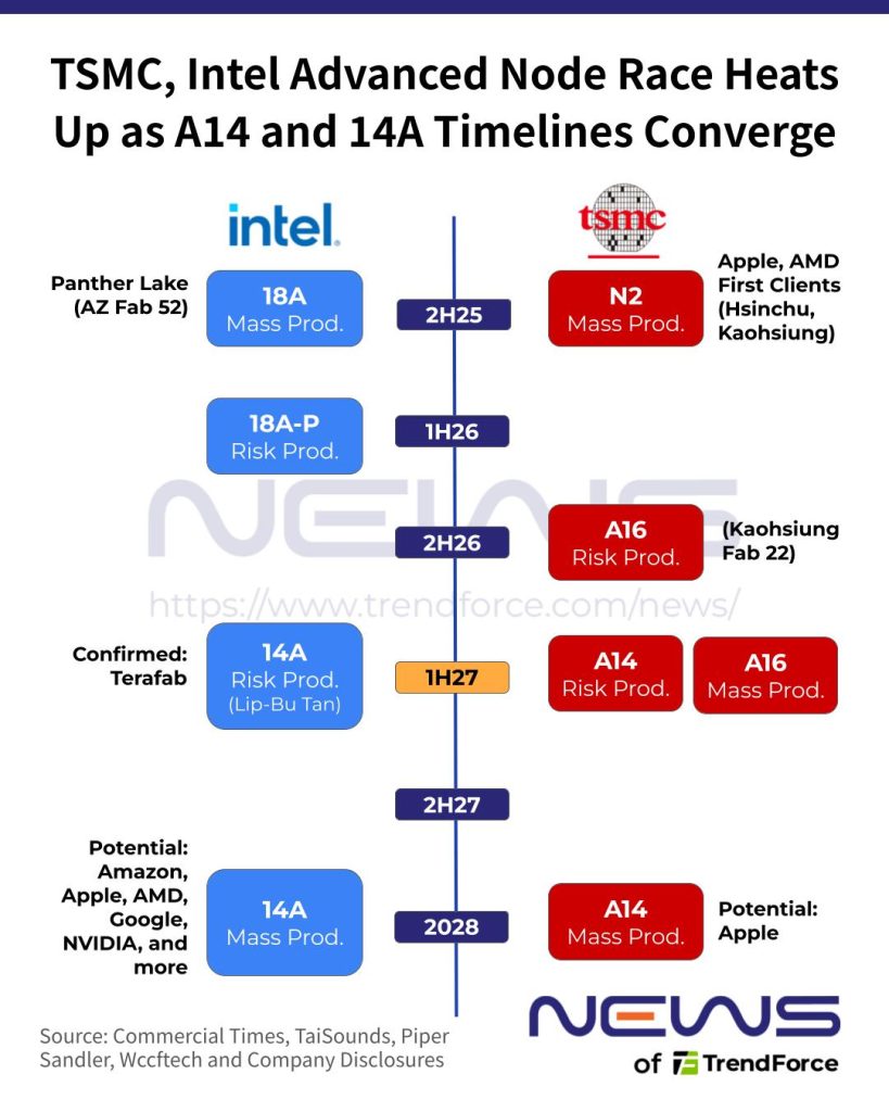
As TSMC prepares for A16 risk production in late 2026, its next-generation A14 node is reportedly running ahead of schedule. Commercial Times, citing IC design sources, says pilot production at Baoshan, Hsinchu, could begin as early as 1Q27—nearly matching Intel’s timeline for bringing 14A into production.
Wccftech reports that Intel CEO Lip-Bu Tan expects 14A risk production in 1Q27, with 18A-P already at that stage. Intel’s official timeline is more conservative, however, targeting 2H27 for internal 14A products and a high-volume ramp in 2028, the report adds.
TSMC’s A14 rollout is already taking shape, keeping its timeline closely aligned with Intel’s 14A push. According to Commercial Times, TSMC launched its A14 CyberShuttle service in 2Q26 and is expected to begin pilot production at Fab 20 in Baoshan. Fab 25 in Taichung, the node’s main production hub, is slated for completion in 2Q27, with pilot runs potentially starting as early as 3Q27, the report suggests.
Process maturity appears to be advancing on both sides of the 14A/A14 race, albeit by different measures. Intel’s 14A defect density had fallen to 0.5 by June 2026, with D0 targeted at 0.1–0.2 by 1Q27, Wccftech reports. TSMC, meanwhile, has reported nearly 90% of target device performance for A14 test vehicles, alongside 256Mb SRAM yields approaching 90%, according to Commercial Times.
As highlighted by Commercial Times, smartphone, HPC, and AI customers are already showing strong engagement for TSMC’s A14, with new design tape-outs running ahead of schedule.
TSMC A14 Takes Shape: Performance and Capacity Plans
For TSMC, A14 carries significant meanings, with MoneyDJ reporting that while unlike A16, which belongs to the 2nm family as a sub-node, A14 is an entirely new process built on second-generation GAAFET nanosheet transistors and the new NanoFlex Pro standard-cell architecture. Compared with N2, A14 is expected to deliver 10–15% higher performance at the same power, or 25–30% lower power at the same speed, while increasing logic density by nearly 20%, MoneyDJ adds.
According to MoneyDJ, TSMC’s combined A14 capacity of Fab 20 in Hsinchu and Fab 25 in Taichung are expected to reach around 60,000 to 70,000 wafers per month. Notably, the report suggests that TSMC also plans to eventually introduce A14 at Fab 22 in Kaohsiung and Fab 21 in the U.S.
Read more
- [News] TSMC Plans Mini-Loop at Kaohsiung to Speed CoWoS Tool Validation; Reportedly Eyes AUO Site for CoPoS
- [News] TSMC Reportedly Targets 22% 2nm, 16%+ 3nm Capacity Boost by Mid-2027; CoWoS to Double by 2028
(Photo credit: TSMC)