


 Facebook
 LinkedIn
 LINE
 Reddit
 WhatsApp
 Kakao

From OCP APAC and Hot Chips in August through SEMICON Taiwan in September, advanced packaging has continued to gain momentum across the semiconductor industry. Why does advanced packaging matter? Transistor scaling is approaching its physical limits, so to maximize efficiency within a single package, the industry is moving rapidly toward chiplet stacking and heterogeneous integration.
TrendForce has long tracked the advanced packaging market. In our previous article, Advanced Packaging: Market Trends and Outlook, we compared TSMC’s CoWoS and Intel’s EMIB, the two mainstream 2.5D technologies, including how they differ and who their main customers are. This article looks at 3D packaging and its key technology, hybrid bonding, and then at the bumpless bonding options beyond hybrid bonding.
Types of advanced packaging: 2.5D, 3D, and 3.5D
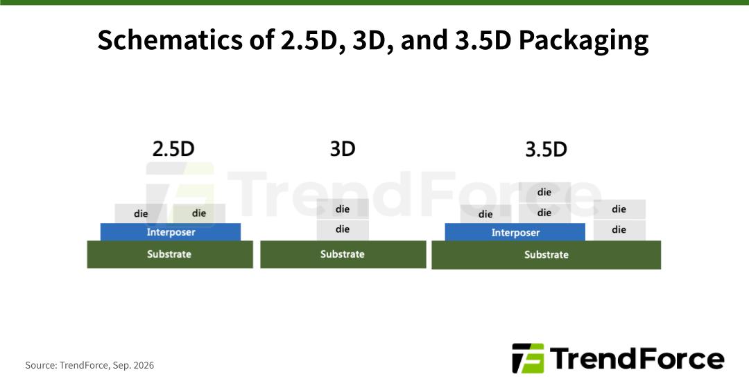
Figure 1. Schematics of 2.5D, 3D, and 3.5D Packaging
Source: TrendForce, Sep. 2026
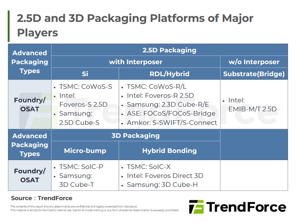
2.5D packaging uses an interposer with extremely high routing density, enabling faster signal transmission and lower power consumption between dies. Examples include TSMC’s CoWoS and Intel’s EMIB (which embeds a small silicon bridge in the substrate instead of using a full interposer).
3D packaging stacks dies vertically to shorten the communication distance between them, as in TSMC’s SoIC and Intel’s Foveros Direct 3D. Both enable an integrated “3.5D” solution that combines 2.5D and 3D packaging in a single architecture. Multiple chips are vertically stacked into a single composite IC, which is then integrated with HBM or other peripheral ICs through 2.5D packaging.
According to TSMC, SoIC with 3D interconnect offers 56x interconnect density and 5x power efficiency over CoWoS with 2.5D interconnect. TSMC commenced mass production of SoIC with a 6µm bond pitch in 2025, and the company expects to further scale SoIC to a 4.5µm pitch by 2029.
On the Intel side, Foveros Direct reached volume production in 1H26 with the Clearwater Forest Xeon 6+ at a 9µm bond pitch. A second generation targeting 3µm is on the roadmap.

CSP ASIC Demand Fuels Advanced Packaging Evolution
CSPs scale ASICs alongside GPUs, lifting packaging demand as CoWoS-L leads while EMIB-T and FOPLP emerge as new options.
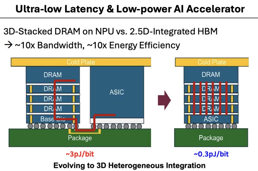
Master the Market TrendsNot only does 3D IC enable logic-on-logic stacking, but it also opens up possibilities for memory-on-logic or logic-on-memory stacking. For example, 3D DRAM architecture places DRAM directly on top of the logic die.
Figure 2. Architecture of 3D DRAM
Source: SK hynix
Building upon the foundation of 3D ICs, the industry is also striving to miniaturize optical components, integrate them into silicon chips, and co-package them with EICs to form optical engines, a technology known as CPO. This paradigm further elevates the complexity of 3D packaging. One example is TSMC’s COUPE, which utilizes hybrid bonding to integrate EICs and PICs. COUPE has been applied in NVIDIA’s Spectrum-X Photonics and Tomahawk 6-Davisson.
ASE has introduced its SiPh Optical Engine, which uses micro-bump technology to vertically bond the EIC and PIC. Intel has launched the OCI (Optical Compute Interconnect) chip that integrates the laser into the PIC, while GlobalFoundries has unveiled the SCALE (Silicon Photonics Co-packaged Advanced Light Engine) platform, which combines FAU and Fiber Array.
For more on CPO, read CPO Testing: The Last Mile to Mass Production.
Why go bumpless
As bump pitch shrinks, bonding in advanced packaging has progressed from flip-chip, suited to bump pitches of roughly 50 µm, to micro-bump plus TCB. Fluxless TCB, which uses no conventional flux, now supports a bump pitch as small as about 8 µm. However, even as thermo-compression technology improves, the micro-bump itself still faces a physical scaling limit. This is what gave rise to bumpless bonding.
Bumpless means no conventional solder balls. Instead, metal on the chip surface, such as Cu pads or under-bump metal (UBM), makes direct contact, allowing smaller interconnects and a bond pitch that can reach around 5 µm. Hybrid bonding is currently the only commercialized bumpless technology. It bonds the dielectric layers and Cu pads of the chips directly through steps such as plasma activation and pre-bonding.
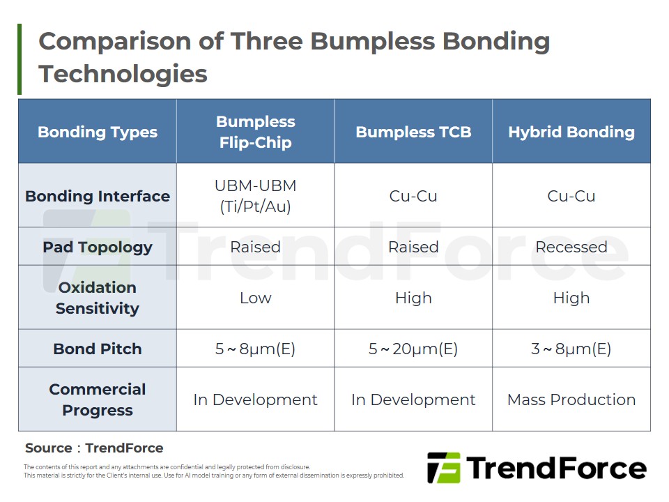
Bumpless Bonding: An Analysis of Alternative Technologies to Hybrid Bonding and Their Market Prospects
Hybrid bonding is costly and cleanroom-intensive. This report compares bumpless bonding alternatives, die bonder roadmaps, and the fluxless TCB market outlook.
Explore the ReportHybrid Bonding Is Costly. Is There a Cheaper Bumpless Option?
The road from micro-bump to hybrid bonding, however, is not a single step. Hybrid bonding comes with high costs and demanding cleanroom requirements, so the industry is still seeking intermediate or complementary options along the way.
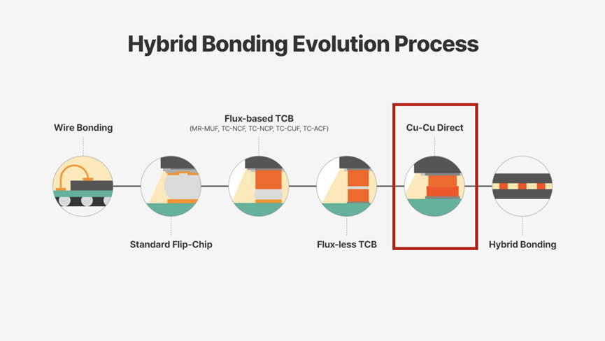
This is why other bumpless bonding technologies are drawing attention. SK hynix’s roadmap, published in August 2026, positions bumpless TCB as an interim step between fluxless TCB and hybrid bonding.
Figure 3. SK hynix bonding technology roadmap from fluxless TCB to bumpless TCB and hybrid bonding
Source: SK hynix; annotated by TrendForce
Want the full analysis? Paid subscribers on TrendForce Substack can read more on:
- Micro-bump + TCB vs. hybrid bonding: how they compare and where each is adopted
- The hybrid bonder supplier landscape: EVG, Besi, ASMPT, and who is closing the gap
- Three challenges beyond bonding, and how the industry is responding
- Two indicators to watch: TSMC’s SoIC capacity plans and changes in Besi’s orders
Bumpless Bonding and Equipment Suppliers
- What drives the cost of hybrid bonding
- How bumpless flip-chip, bumpless TCB, and hybrid bonding compare
- When memory makers could move to bumpless bonding
- How die bonder suppliers are pursuing multiple tracks at once
2026 3D IC Outlook: SoIC Ramp-Up, Rise of STCO
TSMC, ASE, and AMAT spotlight 3D IC at OCP APAC. This report covers 3D IC types, the hybrid bonding process, bonder suppliers, and TSMC's SoIC expansion.
Gain the Full Intelligence