[News] CXMT G5 DRAM Enters Mass Production with 50%+ Higher Dies Per Wafer; SAQP Enables 11.95nm Half-Pitch
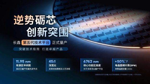
Fresh off announcing LPDDR6 mass production and its debut in Xiaomi’s 18 Fold, CXMT has reached another major milestone. According to Reuters, citing the company’s press release, the Chinese memory giant said its fifth-generation DRAM technology, or G5 Platform, has entered mass production alongside two LPDDR5X products built on the new process.
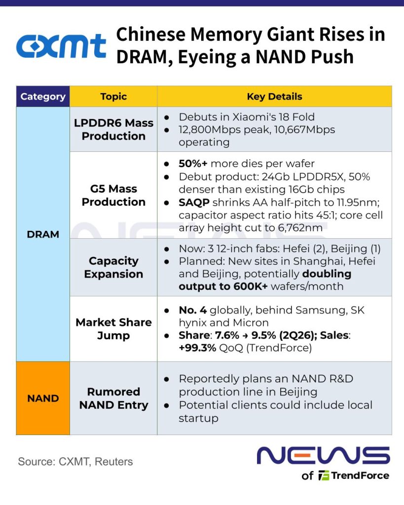
As highlighted by Reuters, CXMT’s G5 Platform’s process scaling has also translated into a substantial gain in die density. Its die-per-wafer (DPW) count is reportedly at least 50% higher than that of the previous-generation platform, helping improve both power efficiency and cost competitiveness.
SAQP Takes Center Stage in CXMT’s G5 Breakthrough
At the heart of G5 is an advanced self-aligned quadruple patterning (SAQP) technique, which has helped shrink the memory array’s active-area (AA) half-pitch to 11.95nm. CXMT says the advance brings its process capabilities closer to the world’s most advanced DRAM techs in volume production.
Notably, SAQP’s significance extends beyond memory. A 2024 Tom’s Hardware report, citing Bloomberg, said Huawei and SMIC had filed patents related to the technique, potentially paving the way for 5nm-class chip production.
For DRAM, the technology is becoming increasingly important as conventional single-exposure DUV lithography approaches its scaling limits. Semiconductor Engineering notes that at advanced nodes such as D1b (1-beta), AA pitches have already narrowed to roughly 22–26nm—beyond what single patterning can achieve. SAQP reportedly addresses that constraint by using multiple spacer-patterning steps to create much finer features.
However, the report notes that added scaling capability comes with greater manufacturing complexity. Small variations in mandrel critical dimension (CD), deposition uniformity, or etching can accumulate through the multi-step process, causing uneven spacing known as pitch walk, the report suggests.
That makes CXMT’s latest milestone particularly notable, as G5 suggests it has moved SAQP beyond development and into volume manufacturing.
On the other hand, process-flow optimization and the integration of new materials have enabled CXMT’s G5 platform to achieve an array-capacitor aspect ratio of 45:1, marking another key step forward in scaling its memory architecture. Meanwhile, by introducing a high-k metal gate (HKMG) process optimized specifically for DRAM, the G5 Platform has reduced its core cell array height to 6,762nm, the company adds.
CXMT Debuts 24Gb LPDDR5X on G5 Platform
Along with the G5 Platform, CXMT also showcased two LPDDR5X products built on the G5 Platform at the 2026 World Manufacturing Convention in Hefei, both offering 24Gb of capacity per die—a 50% increase over comparable products from the previous generation.
Available in 496-ball and 245-ball packages, respectively, the two chips are designed for smartphones and other portable consumer electronics and have already entered mass production, according to CXMT.
Read more
- [News] China’s DRAM Leader CXMT Reportedly Plans NAND R&D Line, Could Challenge Samsung, SK hynix and YMTC
- [News] CXMT Starts LPDDR6 Mass Production at 12,800Mbps; Open to Global Customers as Apple Ties Draw Attention
(Photo credit: CXMT)