[News] Google Marks First 4-TPU Year with 8tx and 8i Max, as 8i Max Doubles HBM Bandwidth to Tackle Memory Wall
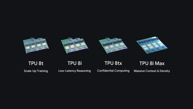
Amid surging AI computing demand and growing uncertainty surrounding market leader NVIDIA, Google is accelerating its TPU expansion. In a November 9 announcement, the tech giant unveiled TPU 8tx and 8i Max, expanding its eighth-generation lineup. According to Newsis, this marks the first time Google has introduced four TPU systems in a single year.
The expansion comes as Google’s custom chips gain commercial momentum. As Reuters notes, TPU sales made a meaningful contribution to Alphabet’s September-quarter results, with Google Cloud revenue more than doubling to $30.71 billion.
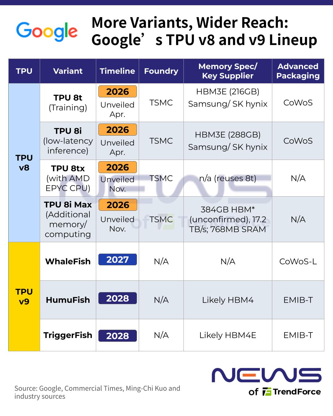
The two newcomers build on April’s TPU 8t and 8i, which deliver up to 2.7x higher training performance and 80% better inference price-performance, respectively, than their predecessors. Dubbed 8tx and 8i Max, the new processors build on existing designs but are optimized for different customer requirements, Reuters adds.
Reuters explains that the 8tx, offering enhanced protection for sensitive information even while data is being processed, integrates Google’s proprietary chip technology with AMD processors, enabling hardware-level data encryption while delivering up to twice the speed of its predecessor with virtually no performance penalty.
TPU 8i Max Takes Aim at AI’s Memory Wall
Google is tackling AI’s growing memory bottleneck with its TPU 8i Max, which combines two existing 8i chips in a single package. According to Newsis, the upgrade raises HBM capacity from 288 GB to 384 GB while doubling memory bandwidth from 8.6 TB/s to 17.2 TB/s, packing more computing power into the same server rack footprint.
As Wccftech notes, the original TPU 8i features 288 GB of HBM3e and 384 MB of on-chip SRAM for active key-value (KV) caching, reducing dependence on external memory. Its servers also swap traditional x86 host CPUs for Google’s Arm-based Axion processors, paired with DDR5 memory for tasks such as data preprocessing.
The dual-chip 8i Max takes this further, doubling compute performance, SRAM capacity to 768 MB, and HBM bandwidth without increasing rack space—effectively delivering twice the compute density, Wccftech adds. However, the report also notes that Google has yet to officially confirm the new chip’s total HBM capacity.
TSMC, Samsung and SK hynix Poised to Gain from Google’s TPU Push
Google’s expanding TPU lineup could bring fresh opportunities for its semiconductor supply chain. According to the Economic Daily News, industry analysts point to TSMC as a key beneficiary, with Google’s eighth-generation chips relying heavily on the foundry giant’s ecosystem, spanning advanced process nodes and system-level packaging.
Memory giants Samsung and SK hynix are also positioned to capitalize on the expansion. As Newsis reports, the two Korean chipmakers reportedly share Google’s HBM3E orders nearly evenly, each accounting for roughly 50% of supply. Notably, analysts expect Samsung’s HBM shipments to Google to double this year, the report adds.
According to News Pim, Samsung Electronics is expanding its collaboration with Broadcom, Google’s TPU development partner, across HBM, foundry services, and advanced packaging. Meanwhile, SK hynix is pursuing joint development of custom HBM optimized for Google’s TPUs, as the two Korean memory giants vie for a stronger foothold in the next-generation AI accelerator supply chain.
Read more
- [News] MediaTek’s Google TPU v9 Shipments May Slip to 1Q28; ASIC Race Heats Up as Taiwan Firms Eye Opportunities
- [News] TSMC’s 3nm Reportedly to Overtake 5nm as Top Revenue Node in 2H26; Output Value Could Top NT$400B
(Photo credit: Google)