[News] Terafab Reportedly Eyes 1M Wafers Monthly by 2032, with 700K for Memory Near Samsung’s Total DRAM Capacity
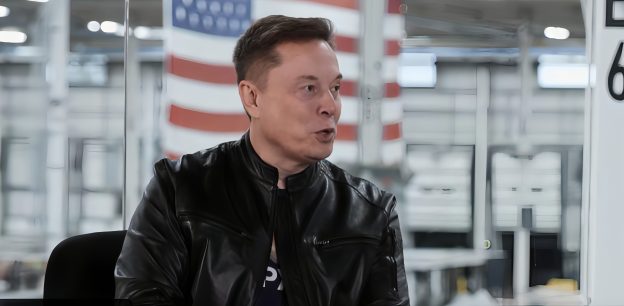
Elon Musk’s Terafab project is reportedly targeting monthly production capacity of around 1 million wafers by 2032. According to Financial News, citing Nikkei, Terafab reportedly told equipment makers this autumn that it plans to produce approximately 700,000 wafers per month for memory chips and more than 300,000 for computing semiconductors. Terafab’s planned total monthly capacity would be roughly 40 times that of Japan’s Rapidus plant in Chitose, Hokkaido, which is designed to produce 25,000 wafers per month, the report adds.
Meanwhile, Wccftech notes that Terafab’s proposed memory capacity alone would be comparable to Samsung’s current total DRAM production capacity of around 650,000 to 700,000 wafers per month. However, details of Terafab’s memory manufacturing plans remain unclear. According to Hankyung, the project has yet to disclose how its planned memory capacity would be allocated between HBM and LPDDR, or whether it would manufacture and stack DRAM chips in-house or rely partly on externally sourced chips for packaging.
Terafab is also reportedly exploring external technical partnerships to support its manufacturing plans. According to Jiji Press, Intel is coordinating technical support for logic chip production, with plans to adopt its 2nm and 1.4nm processes. Citing sources, the report adds that technical cooperation with Taiwanese companies for memory manufacturing is also under consideration, although no specific partners or arrangements have been confirmed.
Terafab is reportedly taking early steps toward equipment procurement. According to Financial News, citing Nikkei, a procurement team reportedly made a confidential visit to Japan earlier this month, seeking deliveries from some manufacturers within months and coordinating equipment installation to support a planned start of mass production in the second half of 2028.
However, significant challenges remain beyond equipment procurement. Financial News notes that advanced semiconductor fabs typically take more than three years to move from construction planning to mass production. Even after equipment installation, additional time is needed to reduce defect rates and achieve stable production.
Tesla’s Reported AI Chip Roadmap Points to Samsung 2nm, Dojo D3 Shift
While Tesla pushes ahead with Terafab, its reported AI chip roadmap suggests the company will continue relying on external foundries for upcoming chips. According to Tom’s Hardware, citing slides purportedly from Tesla, the company’s SI6 inference accelerator is reportedly planned to use Samsung Foundry’s 2nm process, targeting a 2029–2030 launch and up to 80 times the compute performance of HW4.
The reported roadmap also points to a shift in Tesla’s Dojo strategy. After scrapping the original program in August 2025 and announcing plans to revive Dojo 3 in January 2026, Tesla could move away from its earlier SRAM-centric wafer-scale architecture. The next-generation Dojo D3 training accelerator could instead adopt a multi-chiplet design combining 2.5D/3D packaging with stacked HBM, Tom’s Hardware suggests.
Read more
- [News] Musk Targets Terafab Chip Volume Production in 3Q28, First SRAM Test Chip by Mid-2027
- [News] Hanmi Semiconductor Reportedly Receives Terafab Packaging Tool Order, Eyes HBM TC Bonder Supply
(Photo credit: Elon Musk on X)